Latest Posts


YMTC, 128-layer 3D NAND flash memory is officially shipped
Reported by Eefocus on 29 July, according to the official news of domestic storage giant POWEV, its brand Asgard has launched a new product, AN4 PCIe 4.0 SSD, which uses YMTC’s 128-layer 3D NAND flash memory.
The first 3D NAND Flash Memory in China
In October 2017, YMTC successfully designed and manufactured China’s first 3D NAND flash memory. The launch of it is relying on a combination of independent research and international cooperation. In April 2020, YMTC announced its successful development of two 128-layer TLC/QLC products. The X2-6070 model from YMTC is the industry’s first 128-layer QLC flash memory. In addition, it has the industry’s highest IO speed, highest storage density and highest single-chip capacity.
As the industry’s first 128-layer QLC specification 3D NAND flash memory, YMTC X2-6070 has the highest storage density per unit area. Besides it, this model also has the highest I/O transmission speed and the highest capacity among all available models in the industry. The 128-layer 512Gb TLC (3 bit/cell) flash memory chip (model: X2-9060) that is also released this time. This flash chip can meet the needs of different application scenarios.
Xtacking architecture
Thanks to the Xtacking architecture, it has optimized the control circuit and storage unit of 3D NAND. Therefore, YMTC’s 64-layer TLC products have excellent performance in storage density, I/O performance and reliability. The demands in market have raised a lot.
Among the 128-layer products of YMTC, Xtacking has been fully upgraded to 2.0, further releasing the potential of 3D NAND flash memory. In terms of I/O reading and writing performance, both X2-6070 and X2-9060 can achieve a rate of 1.6Gbps (Gigabits/s) under 1.2V. Obviously it is the highest rate in the current industry. Since the peripheral circuit and the storage unit adopt independent manufacturing processes separately, a more high-tech manufacturing process can work with the CMOS circuit. Xtacking 2.0 also brings better scalability for 3D NAND without increasing the chip area.
Through continuous investment in technological innovation, YMTC has successfully developed two 128-layer products and established its technological innovation leadership in the storage industry. With its 1.6Gb/s high-speed reading and writing performance and 1.33Tb high capacity, YMTC has once again proved the forward-looking and maturity of the Xtacking architecture to the industry through X2-6070, and explored a practical path for the future development of the 3D NAND industry.
New Technology – QLC
YMTC claims that QLC is a new technology form of 3D NAND after TLC (3 bit/cell). It has the characteristics of large capacity and high density, and is suitable for reading-intensive applications. Each X2-6070 QLC flash memory chip has a 128-layer three-dimensional stack. Meanwhile, it is with a total of more than 366.5 billion effective charge-trap memory cells. Each memory cell can store 4 bits of data and provide a total of 1.33Tb storage capacity. If you compare the 0 or 1 figure that record data to the small “people” in the digital world. Then you will find out a YMTC 128-layer QLC chip can provide 366.5 billion rooms. Moreover, each room contains 4 “people”, it means approximately a total of 1,466 billion “people” can live here. Thus, its capacity is 5.33 times the capacity of a previous generation single chip with 64 layers.
On July 23, domestic storage device manufacturer Asgard announced the launch of its first PCIe 4.0 SSD product, the model is “AN4”. This solid-state drive is using InnoGrit main control and YMTC domestic flash memory.
It is reported that Asgard AN4 is using YMTC Xtacking 2.0 architecture, 128-layer stacked 3D TLC flash memory chips, and has optional capacities of 512GB, 1TB, and 2TB. Among them, the 1TB version that launched first early August are all with independent cache.
YMTC, 128-layer 3D NAND flash memory is officially on sailing
YMTC has a new development in recent days, or to say it has good news. According to the official news of domestic storage giant POWEV, its brand Asgard launched a new product. AN4 PCIe 4.0 SSD uses YMTC’s 128-layer 3D NAND flash memory. From YMTC’s development of 128-layer 3D NAND flash memory to mass production, and then the launch of Asgard’s new product. It means that YMTC’s 128-layer 3D NAND flash memory has been officially on sailing. For domestic storage that does not currently have high-end PCIe 4.0 SSDs, YMTC has undoubtedly filled this gap.
According to the official introduction, Asgard AN4 adopts YMTC Xtacking 2.0 architecture, 128-layer stacked 3D TLC NAND flash memory chips. The size of them has optional capacities of 512GB, 1TB, and 2TB. Among them, the 1TB version will be emerging in early August, and is using independent cache. The main control solution uses the IG5236 from InnoGrit, which is a flagship solid-state hard drive. SSD in this solution has main control with 8 flash memory channel design and PCIe 4.0 x4 interface.
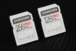
Although PCIe 4.0 has been in the market for two or three years, it still hasn’t become popular yet. The former PCIe 3.0 is still the mainstream in the market. However, Samsung, Western Digital, Seagate, Corsair, ADATA and other manufacturers have all released SSDs that support PCIe 4.0. Industry insiders said that only high-end products in the market will choose to adopt PCIe 4.0.
Main Control chip of SSD
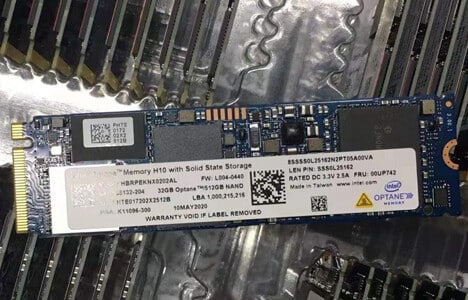
What needs to be briefly clarified is that a complete SSD line needs to have a main control chip, a flash memory chip, and a cache chip. Among them, the cost of flash memory particles account for about 70% of the total cost of the SSD, and determines the capacity of the solid state drive. Also, since flash memory particles have an erasing and writing life, it also determines the ultimate life of the solid state drive. Furthermore, flash memory particles are the ultimate reading and writing objects, so it also have an important impact on speed.
At the same time, the main control chip in an SSD line is the brain of the SSD. It controls the information transmission method of the solid state drive, schedules the access of data in the flash memory particles, and guarantees the lifespan of flash memory through various technical means. Therefore, the main control chip also plays a key role in the performance of the SSD.
How does 128-layer 3D NAND flash memory develop?
With that has been mentioned above, YMTC pioneered Xtacking technology and successfully developed 64-layer 3D NAND flash memory using this technology. Also the mass production for 256Gb (32GB) TLC 3D NAND flash memory had begun in September 2019. Since that many international leading manufacturers have already developed technology that can build NAND flash memory with more than 100-layer. YMTC announced that it will skip the common 96-layer flash memory and directly goes for 128-layer 3D NAND flash memory. Seven months later, in April 2020, YMTC announced that it has successfully developed 128-layer 3D NAND flash memory.
From 32 layers to 64 layers and then to the 128 layers, YMTC has completed its “role change”. YMTC has developed from an industry follower to one of the leading figures in only 3 years. Such a fast change has shocked the industry. POWEV is the first one to launch 128-layer flash memory products. YMTC is a representative domestic IDM manufacturer in the field of flash memory chips, and POWEV is a domestic storage brand giant. Their cooperation has brought many hopes in domestic storage development. It is reported that POWEV is YMTC’s first batch of Xtacking 3D NAND diamond ecological partners.
In addition, this time. InnoGrit is the main control chip supplier for Asgard AN4. InnoGrit is belonging to Marvell. One of the company’s co-founders, Wu Zining, was the global chief technology officer of Marvell. It is reported that the Rainier, which was independently developed by InnoGrit, is the first 12nm PCIe Gen 4 main control chips that have been successfully developed and mass-produced in the world. and it is also the only PCIe Gen4 master chip that has been mass-produced in China.
Who is YMTC
YMTC, whose headquarter is based in Wuhan, China, was established in July 2016. It is a 3D NAND Flash memory chip manufacturer that integrated “development, design and manufacture” (IDM mode). At the same time, YMTC can also provide complete memory solutions for the industry. According to the official website, YMTC has already build R&D centers in Wuhan, Shanghai, Beijing and other places, with more than 6,000 employees worldwide, including about 2,200 senior R&D engineers.
It is worth mentioning that XMC, as a subsidiary of YMTC, has more than 10 years of experience in manufacturing NOR Flash memory. In 2020 alone, the global market size of NOR Flash memory is approximately US$2.3 billion, and the global market size of NAND Flash memory is approximately US$56.6 billion. Therefore, YMTC has business in both NAND flash memory and NOR flash memory. YMTC’s ultimate goal is to become an important part in the global flash memory chip market and supply downstream customers.
YMTC: Will not be directly affected by the judicial procedure of UNIS Group’s bankruptcy and reorganization
On July 16, YMTC said in a statement that unis Group is one of YMTC’s shareholders. However, YMTC has an independent corporate governance structure and has always maintained independent operations. At present, the management team of YMTC is stable. YMTC operates normally, and has abundant capital reserves. The judicial procedure of unis Group’s bankruptcy and reorganization will not directly affect their business activities.
After searched the shareholding structure, we found that the largest shareholder of YMTC is Hubei UNIS Technology Holding Co., Ltd., with a shareholding ratio of 51%. and is indirectly held by unis Group; the second largest shareholder is the National Integrated Circuit Industry Investment Fund Co., Ltd. (National Fund), with a shareholding ratio of 24.1%; the third largest shareholder is Hubei Science and Technology Investment Group Co., Ltd., with a shareholding ratio of 13%; the fourth largest shareholder is Hubei Guoxin Industrial Investment Fund Partnership (Limited Partnership), the shareholding ratio is 12%. The current legal representative of YMTC is Zhao Weiguo, chairman of unis Group.
On July 9th, unis Group issued an announcement stating that the group received a “Notice” from Beijing No. 1 Intermediate People’s Court. The main content was: the relevant creditors claimed that unis Group could not pay off the due debts, the assets were not enough to pay off all the debts and obviously lack the ability to pay off debts. It has reorganization value and reorganization feasibility grounds. Therefore they apply to the court for bankruptcy reorganization of uns Group. The group will fully cooperate with the court to conduct judicial review in accordance with the law, actively promote debt risk mitigation work, and support the court in protecting the lawful rights and interests of creditors in accordance with the law.
Leave a comment