Latest Posts


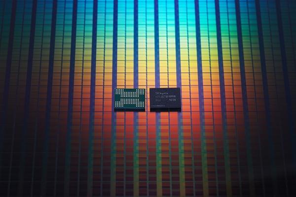
Why micro SD card choose SLC?
At present, the most controversial topic in the industry is the two major architectures of NAND flash, MLC and SLC. The biggest difference between these two architectures is the difference between access technology, which also brings the differences between manufacturing costs, process requirements, auxiliary circuits, and access times. In terms of short-term development, the advantages of the SLC architecture in usage are obvious, and therefore some manufacturers show off their products by mentioning the SLC structure. However, the MLC architecture has the advantages of low cost and a double increase in single-chip capacity compared to SLC. In the long run, MLC will inevitably become the mainstream architecture of NAND flash memory in the next generation. Maybe we are still worry about what architecture the flash memory cards uses when buying portable digital audio and video products, but such concerns will completely disappear in the near future. Why? Let’s see the analysis. but micro sd cards slc still use for Industry and military bc SLC stabilize!
NAND flash memory can be divided into three major architectures, namely Single Level Cell (SLC); Multi Level Cell (MLC); Multi Bit Cell (MBC). MLC was first developed by Intel in September 1997. Its principle is to store two bit information in a floating gate (where flash memory cell stores electric charge), and then use electric charge with different electric potential to control accurate reading and writing function through the voltage control of the memory cell. To put it bluntly, a cell stores multiple bits. The currently common MLC flash memory can store 2 bits per cell, which has twice the capacity of the same SLC architecture chip. Currently, Samsung, Toshiba, Hynix, IMFT (a joint venture company of Intel and Micron) and Renesas are users of this technology. This team is still growing, and its developing speed is much faster than the previous SLC architecture users.
SLC technology has similar principle compared to EEPROM, except that it has thinner oxide film between the floating gate and source gate. It apply voltage to the floating gate’s charge in order to realize data writing. The stored charge can then be eliminated through the source. Every bit of information can be stored in this way. The single-bit method of this technology can provide fast program programming and reading, but this technology limited by the problem of low silicon efficiency, the SLC process technology can only be upgraded upward by more advanced process enhancement technology. At present, it is difficult to make a big breakthrough in single-chip capacity, and it seems to have reached the end of development.
MBC is a NAND architecture jointly developed by Infineon and Saifun Semiconductors using NROM technology. This architecture has not been widely applied due to technical issues. Relevant information on the Internet is also very limited. So, we will not be discussing it this time.
There is a common misunderstanding on the Internet about the two major architectures of MLC and SLC, that is, everyone believes that NAND flash memory with MLC architecture is inferior, and only NAND flash memory with SLC architecture can guarantee quality. However, MLC-based NAND flash memory products have been put into use in 2003. So far, no users have complained about the large-capacity CF and SD cards they purchased have quality problems. Maybe you will say that this is only temporary, and there will definitely be problems in the future, then let’s first recall the development process of MLC and the current SLC development, and then test this assumption.
MLC technology start to become popular when Toshiba launched the first MLC-based NAND Flash in February 2003. At the time, Samsung Electronics, the leading NAND Flash company, was very disdainful of this architecture, and still implemented the SLC architecture vigorously. The next year, in April 2004, Toshiba successively launched 4Gbit and 8Gbit NAND Flash using MLC technology. This is obviously a great news for NAND flash memory, which has gained its reputation for capacity. Samsung Electronics has long advocated the SLC architecture, claiming that SLC is superior to MLC, but the company’s ISSCC papers on MLC technology published in 2004 and 2005 initially show that its views have changed. Samsung has not yet provided any marketing materials about MLC flash memory on its official website, but it has developed a 4Gbit MLC NAND flash memory. The die area of this product is 156mm2, which is 18mm2 larger than Toshiba’s 90nm MLC NAND flash memory. The competition between the two mainstream NAND flash memory manufacturers on the MLC architecture has started from then on. Except from Samsung and Toshiba, IM technology company, which now adopt Intel MLC technology, hope to surpass their competitors in terms of craftsmanship and MLC. The competition for MLC technology is in full swing.
On the other hand, let’s take a look at SLC technology. SLC architecture has two charging values of 0 and 1. That is, each cell can only store1-bit data. It is a bit similar to a switching circuit, very simple but stable, like the CPU part of a computer. If you want to accommodate more transistors in a certain volume, you must improve the level of production technology and reduce the size of a single transistor. At present, SLC technology is limited by the low silicon efficiency problem. To greatly improve the process technology, more advanced process strengthening technology must be used, which means that manufacturers must replace existing production equipment. The investment will be huge. The MLC architecture can store more than 4 charge values at a time, so it has a relatively higher storage density. In addition, the existing production equipment can be used to increase product capacity. Manufacturers enjoy lower production costs and get guaranteed product yields. Therefore, MLC is certainly more popular than the SLC architecture.
Since the MLC architecture is more technologically advanced, and has lower cost and guaranteed yield, then why hasn’t it been accepted by users. In addition to the misunderstandings mentioned above, MLC-based NAND Flash does have disadvantages unbearable for users, but these are only temporary problems. In order to let everyone understand the advantages and disadvantages of these two architectures more intuitively and clearly, let us compare the technical parameters.
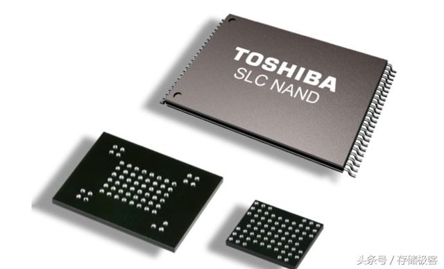
The first is the number of accesses. The MLC architecture can only withstand about 10,000 data writes in theory, while the SLC architecture can withstand about 100,000 times, which is 10 times the MLC. There is also a misunderstanding here. Many media on the Internet have written articles about MLC and SLC, and I have read them one by one. The content is not strict enough. Most of them copy from each other. The mistakes are also exactly the same, which is very irresponsible. Take the number of accesses for example, this 10,000 times refers to the number of data writes, not the total number of data writes plus reads. The number of data reads has a certain impact on the life of the flash memory, but it is not as serious as writing. This life value is changing with the continuous development and improvement of MLC technology. MLC technology is not monopolized by one manufacturer. For example, Toshiba has produced several generations of MLC-based NAND flash memory, including the recently announced 16Gb (2gigabyte) and 8Gb (1gigabyte) MLC NAND that were jointly developed with SanDisk Corporation in the United States, using the most advanced 56nm process. 16Gb flash memory is the largest single-chip capacity in the industry.
Toshiba has experience and technology in MLC flash memory design. Last year Toshiba used 90nm technology to compete with Samsung’s 73nm products. Toshiba’s 90nm MLC flash memory has a bit density of 29 Mbits/mm2, exceeding Samsung’s 73nm flash memory (bit density is 25.8 Mbits/mm2). For a given storage density, Toshiba’s flash memory also has a smaller die area than Samsung’s. For example, Toshiba’s 4-Gbit 90nm NAND has a die area of 138 mm2, while Samsung’s 4-Gbit 73nm NAND has a die area of 156 mm2, which makes Toshiba more competitive in terms of cost. Samsung is now catching up, and its competition with Toshiba is fierce. Coupled with the participation of IMFT, Hynix and other manufacturers, MLC technology has developed rapidly. Today, the writing time of MLC NAND Flash is only 10,000 times, it may rapidly grow to 20,000 times, 30,000 times, and even reach the same level as SLC, which is thousands of times, this is entirely possible in the future.
Let’s compare in term of the write life of MLC NAND Flash. If I recently bought a 2GB capacity MP3 player, the flash memory is Toshiba’s MLC architecture NAND Flash, which can theoretically only withstand about 10,000 data writes. I am a crazy music lover. I have to update the song files in the flash memory every day. In this way, 365 data writes will be performed in a year, so it can be used for at least 27 years. Remove 7 years as data read loss, I can use this MP3 player for at least 20 years if there are no problems with other parts. What does 20 years mean for an electronic product? Even if I cherish old things, it is impossible to use an MP3 player for 20 years. Moreover, even with the SLC architecture, the data retention period in flash memory is only 10 years at most, and 10,000 times of data write is actually a lot.
Followed by reading and writing speed. There is still a misunderstanding here. All flash memory chips read, write, or erase data completed in flash memory control chip. The speed of the flash memory control chip determines the reading, erasing, or rewriting speed in the flash memory. Maybe you will use examples to argue why SLC is faster than MLC under the same control chip and the same peripheral circuits. First of all, I don’t deny this considering of the control technology that the MLC architecture currently uses. But if you understand the inner reasons, you won’t say that SLC has an advantage in speed. SLC technology has been developed much earlier than MLC technology, and the matching control chip technology is very mature. The maximum writing speed of SLC product that I have reviewed can write data at 9664KB/s (KISS KS900), and its reading speed can reach as fast as 13138KB/s (mobiBLU DAH-1700). While the slowest writing speed under the high-speed USB2.0 interface protocol is less than 1500KB/s, and the slowest reading speed does not exceed 2000KB/s. These are all SLC flash chips, all under high-speed USB2.0 interface protocols, but why the differences are so great? I consulted a senior designer in the industry, and the answer was because that the flash memory control chip has low efficiency and poor compatibility with flash memory. Such products are not only slow, but also have a high probability of errors in data operations. This problem also plagued the development of MLC technology when the MLC flash memory was first put on the market. Fortunately, we finally saw some light in December last year. Skymedi Corporation brought us a new generation of high-speed USB2.0 control chip SK6281 and SD 2.0/MMC 4.2 combo flash memory card control chip SK6621, both support MLC NAND flash memory and have good speed performance. The MLC chip it supports has reached the transmission speed of Class4.
For the reasons of Limited by MLC NAND Flash’s own technology, only when the control chip is effective can it support and make up for its shortcomings in speed. Control chips that support the MLC process require stricter standards to fully support the performance of NAND flash chips. After a long-term reliability test and comparison of compatibility of different devices, the series of control chips introduced by Skymedi Corporation have been able to support the current mainstream MLC flash memory, such as Intel JS29F16G08CAMB1, JS29F08G08AAMB1, Samsung K9G4G08U0A, K9G8G08U0M, K9LAG08U0M , K9HBG08U1M, Toshiba TC58NVG2D4CTG00, TC58NVG3D4CTG00, TH58NVG4D4CTG00, Micron, Hynix, etc. In addition, with good firmware design, the performance can be greatly improved to achieve the highest access speed. For example: MLC with SK6621 support can achieve Class4 level, SLC with SK6621 support can achieve Class6 transmission speed. SK6281 also meets the Vista ReadyBoost speed requirement (Enhanced for Windows ReadyBoost), and supports a single MLC with reading speed up to 22MB/s and writing speed up to 6MB/s, which is not much slower than SLC. The slow USB transfer speed of your MP3 player is not all because of the MLC architecture of the flash memory chip, it is more relevant to the control chip.
The third is power consumption. Since the SLC architecture only stores 1 bit of data per cell, there are only two levels of states, high and low, which can be driven with a voltage of 1.8V. The MLC architecture needs to store multiple bits per Cell, that is, the electrical level must be divided into at least 4 levels (stores 2 bits), so it needs a voltage of 3.3V and above to drive. A good news come recently that Intel ’s new 65nm MLC has twice the writing speed compared to previous products, and the operating voltage is only 1.8V. With low power consumption and deep shutdown mode, its battery life has also been extended.
The fourth is the error rate. In one reading and writing, SLC has only two states: 0 or 1. This technology can provide fast program programming and reading. To put it simply, each cell is like a switch used in our daily life. There are only two states: on and off, Very stable. Even if one of the cells is damaged, it will not affect the overall performance. There are four states of MLC in one reading and writing (taking 2bit per cell as an example), which means that the MLC needs to control the charging voltage of each memory cell more precisely when storing, and it needs longer charging time when reading and writing to ensure data reliability. It is no longer a simple switching circuit, but has to control four different states. This has a greater requirement on the error rate and stability of the product. Once an error occurs, it will cause 2 times or more data damage, so MLC has higher requirements on manufacturing processes and control chips. At present, some MP3 main control chips have adopted hardware 4bit ECC check, so that the error rate of MLC and the impact on the performance of the machine can be minimized.
The fifth is manufacturing costs. Why does the production cost remain the same while hard disks keep increase in capacity? To put it simple, it is to store more data on a disk of the same area, which is called the increase in storage density. MLC technology is very similar. Originally, only 1 bit of data was stored in each cell, and now 2 bits or more of data can be stored in each cell. These are implemented without increasing the volume of the memory bank, so MLC NAND with the same capacity has much lower production cost than SLC NAND Flash.
In summary, MLC technology is the development trend of NAND Flash in the future. Just like single-core, dual-core, and quad-core CPUs, MLC technology doubles the capacity by storing more bits per cell until more advanced structure come out. SLC will still be the market leader in the short term, but with the continuous development and improvement of MLC technology, SLC will certainly
Leave a comment