Latest Posts

This article introduces the advantages of 3D NAND compared with 2D NAND and disadvantages of 3D NAND.
3D NAND refers to the memory cell of the flash memory chip is 3D. Previous flash memory mostly belonged to Planar NAND, and 3D NAND, in other words, refers to three-dimensional flash memory. If flat flash is a bungalow, 3D NAND is a tall building. Three-dimensional memory cells mean that the unit area of each memory cell can be significantly reduced. The following picture shows the development of Samsung Planar NAND to 3D NAND (V-NAND).
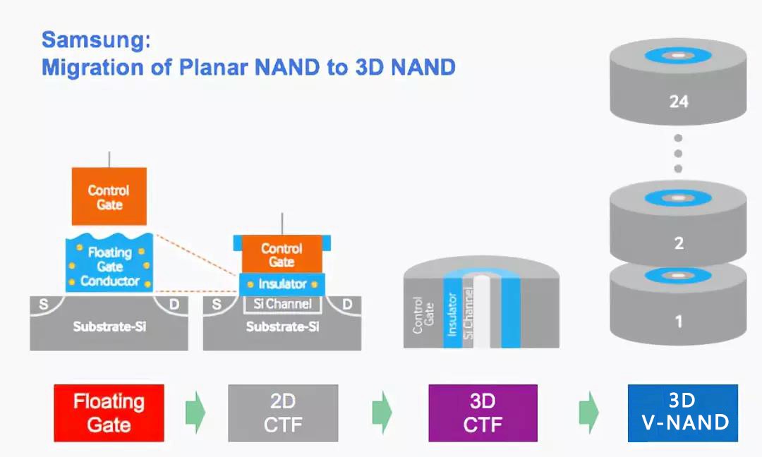
Picture source:Samsung V-NAND technology White Paper (Modified by Author)
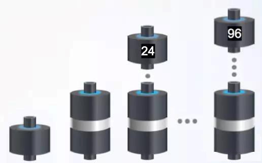
The two on the left are Planar NAND, except that the memory cell structure is different, and the floating gate structure (Floating Gate) migrates to the charge capture flash memory, which is the 2D CTF (Charge Trap Flash) in the above figure. Then, the 2D CTF memory cell 3D is transformed into a 3D CTF memory cell (the 3D CTF in the above figure). Finally, the number of layers of the memory cell is gradually increased by the process technology, and the memory cell is made like a building with more and more layers. The number of 3D V-NAND memory cells in Samsung has gradually increased from 2-layer in 2009 to 24-layer and 64-layer, and reached 96-layer this year.
Picture source : Samsung V-NAND technology White Paper (Modified by Author)
Recently, international original manufacturers have invested in 3D NAND research and development. Each 3D NAND memory unit and technology is different, and almost every company has announced the development of 96-layer 3D NAN.
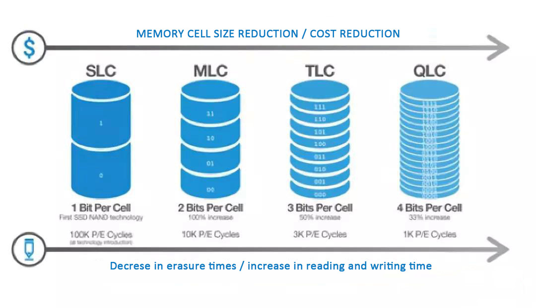
Multi-Level Cell
Generally, normal memory cells, whether DRAM, SRAM, FLASH, ROM, etc., store only one bit of data (called SLC, Single-Level Cell). In order to reduce the size of the memory cell, in addition to the continuous use of the process and the 3D of the memory cell, manufacturers are also actively thinking about increasing the number of bits that can be stored per memory cell. When a memory cell can store two bits (called MLC, Multi-Level Cell), its memory cell size is equivalent to halving. When storing three bits (called TLC, Triple-Level Cell), the size is equal to one third of the original. With four bits (called QLC, quad-level Cell), the memory Cell size is only one quarter of the original size.
SLC stores a bit of data, that is, two states(0,1) ; MLC stores two bits of data, so there are four states (00,01,10,11) ; TLC stores three bits, there are eight states (000,001,010,011,100,101,110,111) ; QLC stores four bits, there are sixteen states (0000,0001,…. 1111), as shown in the figure below.
 Picture source : Micron Official Website (Modified by Author)
There is no such thing as a free lunch. You can’t have your cake and eat it. The cost of reducing the size of memory cell is an increase in design difficulty and a decrease in performance. Why is that? It is also a simple arithmetic problem. Assuming the memory cell voltage is 1.8V, for SLC, one bit has two states, with an average of 1.8V, and each state can be distributed to 0.9V. For MLC, the four states distribute the voltage equally, and each state can be distributed to 0.45v, and so on. TLC can only be distributed to 0.225v for each state, and QLC is even worse, only 0.1125v for each state. Under such a small voltage, many states are separated by very small voltage partition, the smaller the voltage partition is, the harder it is to control, and the more complex the interference is, and these problems will affect the performance, reliability and stability of TLC or QLC flash memory.
As shown in the above figure, the closer to the right, the smaller the relative size of the memory cells, and the lower the cost. However, the Program/Erase Cycle (P/E Cycle, also known as the number of erases and writes) is greatly reduced, and the time required for reading, writing, and erasing is also increased (lower performance). The reduction in the number of erases and writes is quite controversial for this technology, because the number of erases represents the length of life of this flash memory. As shown in the figure above, from SLC to QLC, the number of erases and writes has been reduced from 100,000 to only 1000.
The original manufacturers adopt the systematic design to make up for the shortcoming. By the systematic control of the average number of erases and writes per block, the failed blocks are also replaced by unused blocks to ensure that the flash memory continues to run. Even with only 1000 erases and writes per memory cell, the entire flash memory can still cope with the needs of our daily use. Of course, this result makes TLC or QLC only suitable for personal use by consumers (such as SSD), which cannot meet the needs of enterprises like Data Center, because the frequency of erases and writes in commercial storage devices such as Data Processing Center is quite high.
TSV,Through Silicon Via
TSV technology is not related to the 3D NAND process. Strictly speaking, it is a package technology. It will come out mainly on the one hand, it can make 3D NAND flash memory even higher, and the capacity is increased several times. Another reason is because some people confuse it with the layer level of 3D NAND memory cells, which describe 32, 64 or 96-layer 3D NAND as stacking 32, 64 or 96 grains(Die). This is a big misunderstanding.
TSV technology is widely used in DRAM and Flash products. In the past, an IC chip packaged only one grain, and in order to reduce cost, save board space and improve performance, multi-chip packages (MCP) began to flourish (as shown on the left in the figure below). TSV is a process of perforating the IC substrate, filling the metal, allowing the upper and lower grains to be directly connected (as shown on the right in the figure below), which can not only eliminate the package line shown in the left figure (Bonding) ), but also further enhance the capacity, signal quality, transmission performance of DRAM or Flash single chip, and reduce conducted noise interference.
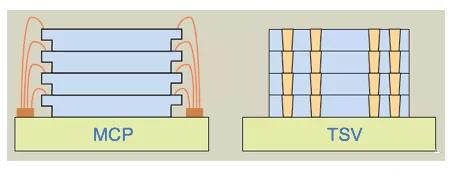
Picture source:3D NAND Flash Memory – Toshiba (Modified by Author)
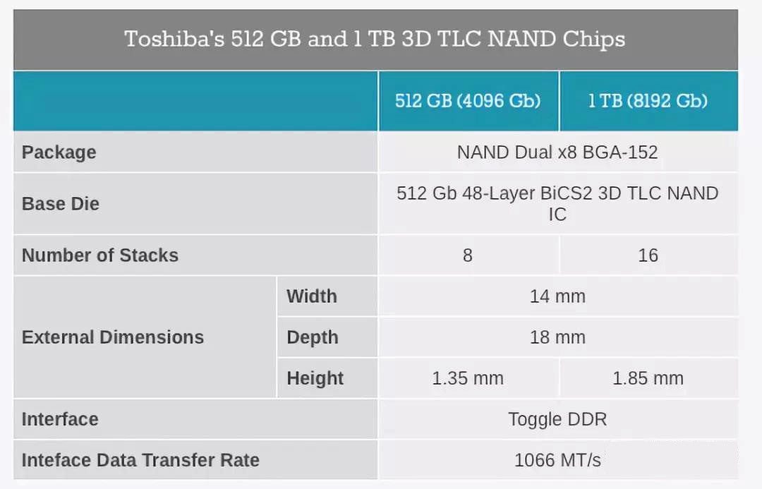
Now, most of the mass-produced 3D NAND chips are stacked in TSV to 8 or 16 layers of 3D NAND grains . The following table shows an example of Toshiba’s 512GB (Gigabyte)/1TB (Terabyte) flash memory. You can clearly see that it uses a 48-layer 3D NAND memory process to create a 512 Gb (Gigabit) flash memory grains. TSV technology stacks 8 or 16 (Number of Stacks in the following table to indicate the number of stacks) to make 512 GB (512Gb x 8) or 1TB (512Gb x 16) flash memory chips. (Note: lowercase b stands for bit (bit), uppercase B stands for byte (byte), and a byte equals 8 bits).
Picture source:AnandTech Post : Toshiba Weds 3D NAND and TSV
So, a grain of NAND flash, using 3D NAND technology, can stack up to 96-layer storage units, like a skyscraper. In order to increase the capacity of each packaged chip, the manufacturer then stacks 8 or 16 dies into TSV technology to package them into chips.
Leave a comment