Latest Posts


Traditional storage technology facing challenges pushes the emergence of new one
Regarding the memory chip, its process is relatively simple and memory cells can be quickly replicated, so that it can help advanced process technology to rapidly improve the yield. For a long time, memory chip has been the first person with courage to try something new for advanced manufacturing processes. However, with advanced process technology entering 65-nm era, a considerable number of advanced process manufacturers have accumulated enough experience to omit memory verification and directly apply advanced process to logical products.
When the rise of AI, Internet of things and other fields makes the application of big data more and more extensive, these emerging fields are constantly urging memory to catch up with advanced process. At present, even though the major memory card manufacturers are upgrading 20nm process, traditional memory such as DRAM, bulk micro SD memory card, NAND flash and SRAM is still the main technology on the market.
In this process, traditional storage technology encounters many difficulties. For instance, DRAM with continuously miniaturized cell design requires introducing multi-pattern technology, and ultimately using EUV lithography technology in mass production, while we all know that EUV has not been able to be applied on a large scale. Similarly, faced with the limitation of miniaturization, planar NAND finally takes a vertical shift, resulting in very popular 3D NAND technology on the market now.
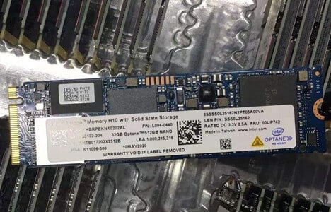
Traditional storage technology such as SD Card in bulk is facing challenges; on the contrary, it is giving rise to the emergence of new technologies, for example MRAM. MRAM has high-speed reading and writing performance of SRAM and high integration of DRAM, along with basically repeating writes indefinitely. In other words, after combining the density of memory with the speed of SRAM, MRAM is non-volatile and highly effective.
MRAM technology had begun in 1984, when Albert Fert and PeterGrünberg discovered GMR effect. In the mid-1980s, proponents argued that MRAM would eventually become dominant or even universal memory. In 1996, the spin transfer torque was proposed, a finding that allows magnetic tunnel junctions or spin valves to be modified by spin polarization currents. Based on this, Motorola began to do research on MRAM. One year later, Motorola developed a 256Kb MRAM test chip, which marked the beginning of MRAM technology. In 2002, Motorola was awarded a patent to Toggle, which was the first generation of MRAM and called as Toggle MRAM. However, even under advanced process nodes, high-energy consumption of the first generation of MRAM hindered the development of MRAM.
In 2004, Motorola spun off its semiconductor business to form Freescale semiconductor. In July 2006, Freescale began selling the world’s first commercial MRAM chip at $25, with a capacity of as low as 4M bits. At this time, MRAM started to attract the attention of other manufacturers, including infineon, TSMC, Toshiba, and Renesas. Generally, MRAM technology was developed to the second generation. At present, the mainstream is TAS-MRAM and STT-MRAM.
One of the second generation of MRAM devices is SST-MRAM, using spin polarization currents to switch electron spins. In 2005, Renesas collaborated with Grandis to develop a 65nm SST-MRAM that was faster, more efficient and easier to shrink than MRAM. Compared with traditional memory technology, SST-MRAM can not only take into account the performance of MRAM, but also meet the requirements of low current and lower cost.
Based on these advantages above, SST-MRAM is regarded as a high-performance memory that is better than DRAM and SRAM, and has the potential to become a leading storage technology. Especially in the process nodes below 40nm, when NOR began to expose many problems, SST-MRAM was highly expected. The industry believes that STT-MRAM can be utilized not only at 40nm node, but also below 10nm. What’s more noteworthy is that STT-MRAM can be developed, with the help of the existing CMOS manufacturing technology and process. It is relatively easy to inherit various technologies, so STT-MRAM can directly challenge the low cost of flash.
The dream is plump but the reality is skinny. As the technology scale shrinks, STT-MRAM suffers from severe process changes and thermal fluctuations, which greatly reduces its performance and stability. Thus, STT-MRAM still has a long and hard way to go for most commercial applications.
Structurally, the core of STT-MRAM storage cell is a MTJ, that is, STT-MRAM stores data through MTJ. MTJ is composed of two layers of ferromagnetic layer with different thickness and a layer of non-magnetic isolation layer. When writing data, a large current is needed to generate a magnetic field to reverse the magnetic moment of MTJ free layer. As the size of the storage cell decreases, a larger magnetic field is required to reverse the magnetic moment of MTJ free layer. Larger magnetic field requires larger current. However, the large current not only increases the power consumption, but also slows down the conversion speed, further limiting writing speed of storage cell.
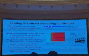
At CSTIC 2019, some experts mentioned that the current challenges of STT-MRAM mainly focused on the balance between large write current, MTJ scaling and the reduction of bit error rate.
Challenges also represent opportunities, and STT-MRAM remains attractive to major manufacturers. In 2008, Freescale spun off its MRAM business into Everspin Technologies. In 2014, Everspin partnered with Global Foundries to produce in-plane and vertical MTJ STT-MRAM on 300mm wafers, using 40-nm and 28-nm node processes. In 2017, Everspin was famous as the only company to ship commercial MRAM products, indirectly reflecting Everspin’s great strength in this area. In 2018, Everspin also worked with Global Foundries to launch the world’s first 28 nm 1 Gb STT-MRAM customer sample. As we all know, Global Foundries has stopped investing in 7nm below advanced manufacturing process, instead 14nm or 12nm FinFET. However, the market expectation for STT-MRAM does not remain at 12nm. Next, which OEM will Everspin choose to cooperate with?
Let’s trace back to ten years ago. SK Hynix semiconductor and Grandis started their partnership in 2008 to explore the commercial development of STT-MRAM technology.
As mentioned above, Renesas also cooperated with Grandis in STT-MRAM. Was Grandis able to gain a foothold in the storage field with emerging technologies? Grandis, founded in 2002, invented the first spin transfer torque film structure based on magnetic tunnel junction, and quickly became the leader in the field of STT-MRAM. Grandis was acquired by Samsung Electronics in 2011 and incorporated into Samsung’s memory business. As a result, Samsung intended to develop STT-MRAM. During wafer foundry forum in 2018, Samsung Electronics reiterated its goal of starting production of STT-MRAM chips and announced the real STT-MRAM mass production would begin in 2019.
In addition to Grandis, IBM is also a pioneer of STT-MRAM, working with Infineon and Samsung. In 2016, IBM and Samsung demonstrated 11-nm STT-MRAM. In 2018, IBM showed off FlashCore NVMe SSD, which provided 19TB flash memory and utilized Everspin’s 5-256Mb STT-MRAM chip for writing caching and logging.
According to Yole’s survey during CSTIC 2019, besides Global Foundries and Samsung mentioned above, top fabs including TSMC, Intel and UMC have been ready to use 28/22nm embedded STT-MRAM for microcontrollers.
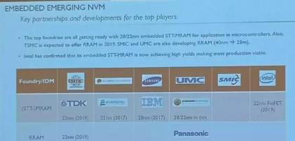
Intel revealed that it intended to make STT-MRAM technology mass production at the International Solid State Circuits Conference in the United Kingdom in February 2019. It’s reported that Intel expected to produce memory chips by using 22-nm FinFET process.
In 2000, TSMC cooperated with Industrial Technology Research Institute of Taiwan to invest in MRAM research and development. In 2011, Qualcomm also demonstrated 1 Mbit embedded STT-MRAM using TSMC 45nm LP technology at the VLSI Seminar. TSMC gave up developing MRAM because of cost, but in 2017 TSMC re-targeted MRAM and RRAM. According to DIGITIMES, TSMC is highly likely to produce massive STT-MRAM in 2019.
Similarly, UMC and Avalanche Technology announced that they have jointly developed and produced 28nm MRAM to replace embedded flash in 2018. UMC also provided this technology to other companies through a license from Avalanche Technology Inc.
For Chinese mainland, GigaDevice spent $5 million on buying a share of Everspin in 2016. In 2017, the first 80nm STT-MRAM device in China was prepared successfully by Beihang University and Institute of Microelectronics of the Chinese Academy of Sciences (IMECAS). Zhao Chao, a researcher in Integratd Circuit Advanced Process R&D Center of IMECAS, and Zhao Weisheng, a professor in Beihang University, made an important breakthrough in key technology research of STT – MRAM. It’s for the first time that China successfully prepared 80nm-diameter magnetic tunnel junction with good performance by adopting compatible CMOS process. For instance, tunneling reluctance, one of the core parameters of magnetic tunnel junction, can reach at 92%.
Shanghai Ciyu is the first Chinese company fully dedicated to develop and deliver revolutionary products with disruptive PSTT-MRAMMRAM technologies and 12 pilot lines under construction, which will be used for developing and manufacturing the third and fourth generation MRAM memory chips. Its team members come from Everspin and TDK. Ciyu invests on standalone and embedded technology strategies on the market.
Zhejiang Hikstor also focuses on the development of MRAM technology. Its team members are from Qualcomm, Western Digital and other international semiconductor manufacturers. At present, Hikstor has invested on chip design and process design, and can provide different equipment for STT-MRAM technology.
It can be seen that even though major wafer factories are planning to massive production of STT-MRAM in 2019 and gradually moving towards 28nm below products, Chinese mainland still struggles with 40nm above STT-MRAM. The emergence of STT-MRAM makes international manufacturers shift their attention from NOR. However, recently, some professors have reported on Semicon China 2019 that it would take a long time for STT-MRAM to completely replace NOR technology, and that this time difference will provide an opportunity for the mainland to develop NOR.


Leave a comment