Latest Posts


SLC vs. MLC nand Flash introdaction and what’s their differences
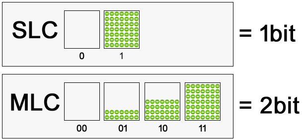
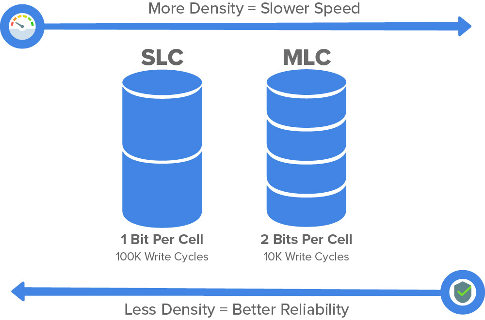
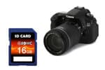
There are two types of storage cells: SLC (single layer cell) and MLC (multi-level cell). SLC is of high cost, small capacity and fast speed, while MLC is of large capacity, low cost, but slow speed. Each unit of MLC is of 2 bits, which is twice as many as that of SLC. However, the large amount of data stored in each MLC storage unit that has a relatively complex structure increases the probability of error. So, error correction must be carried out, which leads to its performance inferior to that of SLC that has a simple structure. Another advantage of SLC is its up to 100,000 write cycles, 10 times higher than MLC flash memory. In order to ensure the service life of MLC, the control chip must perform the checksum intelligent wear-leveling algorithm, so that the write cycles of each storage unit can be evenly apportioned, reaching 1-million-hour mean time between failures (MTBF).
A common misunderstanding online about MLC and SLC architectures is the NAND flash memory of MLC architecture is inferior and that only the NAND flash memory of SLC architecture has assured quality. As everyone knows, market introduction of NAND flash memory products with MLC architecture started as early as 2003. So far, no user has complained about the quality of the large-capacity CF and SD cards that he or she has purchased. You may say this is temporary and that there will definitely be problems in the future. So, let us recall the MLC history and study the current status of SLC before drawing a conclusion.
MLC technology became known in Feb. 2003 when Toshiba launched its first MLC architecture NAND flash product. Samsung Electronics, the leading enterprise of NAND flash products at the time, disregarded the Toshiba product and went its own way promoting the SLC architecture. In April 2004, Toshiba successively launched 4GBIT and 8GBIT NAND flash products using MLC technology, which made its large-capacity NAND flash products even more powerful. Samsung Electronics had long advocated SLC architecture, claiming that SLC is superior to MLC. But the ISSCC papers on MLC technology the company published in 2004 and 2005 initially showed a shift in its view.
Without providing any relevant marketing information on its website, Samsung now had developed a 4GBIT MLC NAND flash product. The size of its die is 156mm2, 18mm2 larger than that of the Toshiba 90nm MLC NAND flash chip. The competition between the two major manufacturers began. In addition to Samsung and Toshiba, the IM technology company, a later comer that had acquired the Intel MLC technology, aspired to surpass its competitors. The competition for MLC technology was in full swing.
On the other hand, let’s take a look at SLC technology. In principle, the SLC architecture has two charging values of 0 and 1, i.e., each cell can only access 1 bit of data, which is somewhat similar to the switching circuit, simple but very stable. Like with the CPU of a computer, if you want to accommodate more transistors in a certain space, you must improve the production process to reduce the transistor size. At present, the SLC technology is limited by the problem of low silicon efficiency. In order to greatly improve the process technology, more advanced process-enhancement techniques must be adopted, which means manufacturers must replace the existing equipment with investment that could be large and bottomless. The MLC architecture can store more than 4 charging values at a time, hence a better storage density. Furthermore, the existing equipment can be used to improve the product capacity, so that the manufacturers can enjoy the advantage of production cost and assured quality of the products.Therefore, MLC architecture is better than the SLC one.
The MLC architecture is more advanced in technology and has the advantages of cost and yield. But why was it not recognized by users for a long time? Apart from people’s misunderstanding, the MLC architecture NAND flash does have some shortcomings that users can’t tolerate. But that will not last long. Let’s compare their technical parameters to let you have a clearer understanding of the advantages and disadvantages of the two architectures.
As for the number of accesses, the MLC architecture can theoretically only withstand about 10,000 data writes, while SLC architecture can withstand about 100,000, 10 times that of the MLC. But there is also a misunderstanding here. Take the number of accesses as an example. This 10,000 times refers to the number of data writes, not the total number of data writes and reads. The number of data reads has a certain impact on the service life of a flash memory chip, but it is not as serious as the writes. The MLC life value is improving with the continuous development of the technology. MLC technology is not a monopoly of any manufacturer. Toshiba, for example, has made several generations of MLC architecture NAND flash chips, including the 16GB (2gigabyte) and 8GB (1gigabyte) MLC NAND flash chips that were jointly developed with the SanDisk company of the United States using the most advanced 56nm process. 16GB so far is the largest capacity of a single chip.
Toshiba is experienced and has the technology in MLC flash memory design. Last year, it used 90nm process to compete with Samsung’s 73nm products. Its 90nm MLC flash chip has a bit density of 29 Mbits / mm2, exceeding Samsung’s 73nm flash chip (with a bit density of 25.8 Mbits / mm2). For a given storage density, Toshiba’s flash chip also has a smaller die area than Samsung’s. For example, Toshiba’s 4-gbit 90nm NAND die area is 138 mm2, while Samsung’s 4-gbit 73nm NAND die area is 156 mm2, which makes Toshiba more competitive in terms of cost. Samsung is catching up, however, and the competition between the two has got extraordinarily heated. With IMFT, Hynix and other manufacturers joining in the contest, MLC technology is developing rapidly. Today, a MLC NAND flash chip has only 10,000 write cycles, and tomorrow it may get to 20,000, 30,000, or even 100,000 write cycles, which is the same level as SLC. Nothing is impossible.
Let’s do a calculation based on the write cycles of a MLC NAND flash chip. Suppose this writer recently purchased a 2GB MP3 player with a Toshiba MLC NAND flash chip which can only withstand about 10,000 data writes in theory. This writer is a crazy music lover and updates the song files in the flash chip every day. So, 365 data writes will be performed in one year, and 10,000 write cycles are sufficient for me to use it for at least 27 years. Removing 7 years as the loss of the life of the flash chip caused by data read, I could still use this MP3 player normally for at least 20 years if no problem occurs with its other parts. What does 20 years mean to an electronic product? No one could use a MP3 player for 20 years. Even if with the SLC architecture, the data storage life of a flash chip is 10 years at most. So, the 10,000 write cycles is actually a sufficiently large number.
The second thing I will talk about is the read and write speed. There is a misunderstanding here. Data read-write-erase is controlled by the flash memory control chip. The speed of the control chip determines the speed of the data read-write-erase. You may use ready-made examples to argue why SLC is faster than MLC under the same control chip and the same peripheral circuit. I don’t want to deny that the MLC is slower than SLC because of its structure and control technology. But if you know the truth, you won’t say that SLC has advantages in speed. The SLC technology was developed much earlier than MLC technology, and its control chip technology is mature. According to my own test, the fastest write speed of a SLC product can reach 9664kb/s (KISS KS900), and the fastest read speed can reach 13138kb/s (mobiBLU DAH-1700). Meanwhile, under the same high-speed USB2.0 interface protocol, its slowest write speed is less than 1500KB/s, and the slowest read speed is no more than 2000KB/s.
Why does a SLC flash memory chip with high-speed USB2.0 interface protocol have such a different performance? This writer consulted a senior designer in the industry, and the answer is that the efficiency of the control chip is low, and its compatibility with the flash chip is not good. This kind of product is not only slow, but also has a high probability of error in data operation. This problem has also plagued the development of MLC technology since the MLC flash chips were launched. Fortunately, we saw the silver lining last December when the Skymedi Corporation launched a new generation of high-speed USB2.0 control chip SK6281 and SD 2.0/MMC 4.2 combo flash memory card control chip SK6621. They both perform well in MLC NAND flash memory support and speed. The MLC chips they support have reached the transmission speed of class 4. The MLC NAND flash chip can make up for its poor speed with a control chip that has high efficiency. The control chip supporting the MLC process requires strict standards to give full play to the performance of NAND flash chip.
With many reliability tests and comparison calibrations for compatibility of different devices, the control chips launched by Skymedi have been able to support the mainstream MLC flash memory chips in the market, such as the Intel JS29F16G08CAMB1 and JS29F08G08AAMB1, the Samsung K9G4G08U0A, K9G8G08U0M, K9LAG08U0M and K9HBG08U1M, the Toshiba TC58NVG2D4CTG00, TC58NVG3D4CTG00 and TH58NVG4D4CTG00, and products from Micron and Hynix and others. In addition, Skymedi products’ good firmware design can help improve the performance and access speed of flash chips. For example, the SK6621 can push MLC to the speed level of class 4, and can increase SLC’s speed to class 6. Meanwhile, the Sk6281 meets the speed requirements of Vista ReadyBoost (enhanced for windows ReadyBoost) and can help a single MLC achieve the read speed of 22mb/s and the write speed of 6MB/s, which is not much slower than SLC. So, the slow USB transmission speed of your MP3 player is not all because of the flash memory chip adopting the MLC architecture. It is more related to the control chip.
The third thing I will talk about is power consumption. The SLC architecture only stores 1 bit of data per cell, so there are only two levels: high and low. It can be driven with a voltage of 1.8V. The MLC architecture needs to store multiple bits per cell, i.e., the level must be divided into at least four levels (storing 2bit), so it needs a voltage of 3.3V or above to drive. There is good news now. The write speed of Intel’s new 65nm MLC is twice that of previous products, with the working voltage of only 1.8V. Low power consumption and the deep shutdown mode has also extended the battery life.
The fourth is the error rate. In one read-write, SLC has only two states: 0 or 1. This technology enables fast programming and read. In short, each cell is like a switch used in our daily life. It has only two states: on and off. It is very stable. Even if one cell is damaged, it will not affect the overall performance. MLC has four states in one read and write (taking 2bit access per cell as an example), which means that the charging voltage of each storage unit should be more accurately controlled during MLC storage, and longer charging time is required to ensure the reliability of data during read and write. It is not a simple switching circuit. It is to control four different states and has strict requirements concerning product error rate and stability. Once an error occurs, it will lead to 2 times or more data damage. Therefore, MLC has higher requirements for manufacturing process and control chip. At present, some MP3 main control chips have adopted hardware 4bit ECC verification, which can minimize the error rate of MLC and the impact on machine performance.
The fifth is the manufacturing cost. Why can the production cost remain unchanged while the capacity of hard disk has increased exponentially? Simply put, more data can be stored in the same area of a cell, or the storage density has increased. MLC has similar technology. Originally, only 1 bit of data was stored per cell, but now each cell can store 2 bits or more data, with the cell size remaining unchanged. So, the manufacturing cost of a MLC NAND flash chip with the same capacity is much lower than that of a SLC NAND flash chip.
To sum up, MLC technology represents the future of NAND flash chips. Just like CPU single core, dual cores and four cores, MLC technology can double its capacity by storing more bits per cell, while waiting for emergence of a more advanced architecture. Although SLC will remain the market leader in the near future, it will fade away with the continuous improvement of the MLC technology.
Copyright statement: This article is the original article by CSDN blogger “seable” and follows the CC 4.0 by-sa copyright agreement. For reprint, please attach the source link of the original text and this statement.
Leave a comment