Latest Posts


How production process for MICRO SD Cards by Wafers?
With the application of bulk Micro SD Card in the field of GPS, Drone, Dash cam, Sport camera, Raspberry Pi and Mobile phones is becoming more and more common, these device manufacturers and consumers have higher and higher requirements for the quality of wholesale Micro SD cards . Refer to the popularity of micro SD card; it has successfully climbed to the throne of best storage accessory. So how does micro SD come into being?
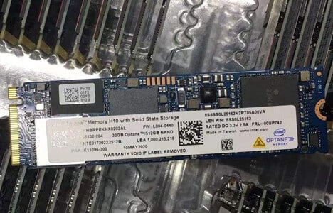
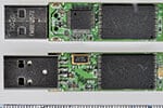
The production process of micro SD is basically following this way, the manufacturer purchases the core component of the memory card from the upstream wafer supplier, and then they carry on the cutting test on the wafers, and they will stack the cutting wafers. With these cutting wafers, they will weld the circuit board, controller and the other parts together on the substrate, finally they will do package to complete the finished product — micro SD in bulk.
As the smallest type of memory card, the enviable volume advantage is bound to associate with high technical threshold. At present, there are few manufacturers in the world that can make large capacity micro SD in mass production.
When it comes to memory cards, it is not the shell that plays a decisive role in its function, but the flash memory chip; in other words, it is the well-packaged cutting wafer. Without the flash chip, the memory card is like an old saying “Water without a source, and a tree without roots.” and it is useless at all. This means that if any one hope have the ability to make micro SD cards in mass production, they must firstly have the ability to obtain high-tech wafers, and ensure the stability and sustainability of wafer supply. In fact, now many OEM factories such as MRT technology has a good cooperative relationship with the major upstream wafer suppliers, with the strong support of these suppliers, MRT technology has a solid raw material foundation. This is a prerequisite for a memory card manufacturer to support mass production of micro SD cards. This is a combination of strong upstream and downstream integration capabilities, only manufacturers who reach this level can take the lead in the fierce memory card competition.
To produce the memory card as small as micro SD, the wafer is the premise, and the packaging and testing technology is the key. This kind of memory card, which is thin in shape and small in size, it can not be assembled in the way that most manufacturers did for Bulk SD memory cards or USB drives, only when the factory has the ability to do COB way. This means that micro SD cards have brought memory cards into a new era of semiconductor packaging. The components (controller, flash memory integrated circuit, basic material, passive computing element) needed by the small memory card are encapsulated directly to form the finished memory card. This technology is used in the field of Micro SD Card production is like a duck in water, it makes the production of high-capacity micro SD card easier, and all the Micro SD Cards is real under the application of PIP packaging technology, also the cards will be completely waterproof, pressure and folding resistance.
We cannot ignore the stacking technology when producing micro SD cards. With stacking technology, micro SD can be more powerful leading a big step forward higher capacity. Because of the volume, the chips of micro SD cards can not be placed in parallel, such as SD cards and MMC cards, but they need to stack two or more chips and connect them with complex lines. The production process for micro SD card is highly hard to reach perfect without stacking technology, as it requests extremely high technology to stack chips and make lines do series connection in such tiny volume, so no one can finish it unless the manufacturer can do semiconductor packaging. At the same time, because of the advanced stacking technology, NAND Flash Manufacturer can use larger SLC wafers to produce large capacity micro SD, which makes their micro SD three times faster than most micro SD products made by MLC in the market, the speed can reach 10m/s; meanwhile it can be erased more than 100000 times. Its low working voltage reduces the power consumption and extends the life circle of Micro SD Card.
In addition, the shape of micro SD card has irregular cutting angle, it needs to use special machine and technology to cut, and this also set the technical threshold for many manufacturers. The huge investment in equipment and technological innovation breakthrough of NAND Chip Manufacturer has greatly improved the efficiency and production capacity, and successfully got rid of the shackles of cutting angle.
With the help of the rich entertainment function of mobile phones, the high storage demands of GPS, Dash cam and Drone, micro SD cards have been more and more popular in the memory card market, and many manufacturers are eager to share this huge market. However, under the constraints of very high technical threshold, only the manufacturers possess with their own packaging and testing capabilities, then they can occupy one place in the fierce competition and establish their own storage kingdom!
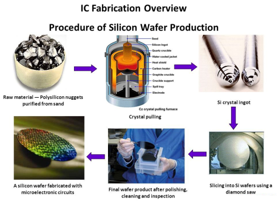
In order to know further about the production process of MICRO SD card, we need to know what is wafer. Wafer (Wafer) refers to the silicon wafer used in the fabrication of silicon semiconductor integrated circuits; one piece of wafer can be cut into thousands of chips.What is a wafer? Wafer (Wafer) refers to the silicon wafer used in the fabrication of silicon semiconductor integrated circuits. Because of its circular shape, it is called round wafer, and also known as crystal elements or silicon wafers. Wafer is widely used in the field of electronic digital such as Memory bank, SSD, CPU, video card, Micro SD Card, SD Card, USB Drive, mobile phone fingerprint chip and so on, it can be said that almost all electronic digital products needs wafer, it means wafer is indispensable. Therefore, in recent years, the shortage of global wafers has not only led to the increase in the price of memory storage and SSD but also the cost of whole field of electronic digital products. It is the importance of the wafer. The refining and cutting of wafer The main raw material of wafer is silicon, the rise of “Silicon Valley” in the United States started from the semiconductor industry at that time, so it has the name of “Silicon Valley”.
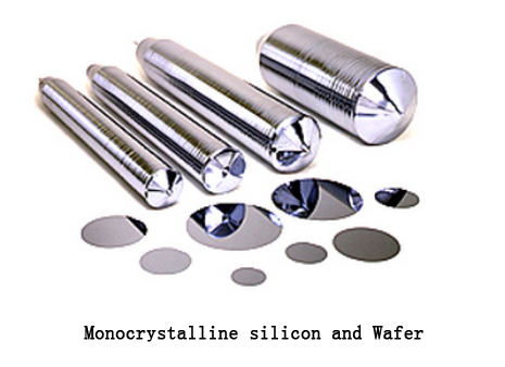
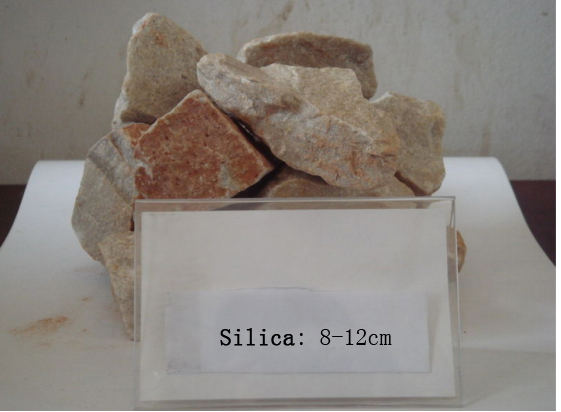
Silicon is one common substance, and the sand we see in daily life is full of silica. The sand can be turned to Monocrystalline silicon if it gets purified many times, also the whole process is operated under the high temperatures, and becomes cylinder after the way of rotating and stretching. The Monocrystalline silicon weighs about 100 kilograms.
If we can get silicon from the sand, then we can get them easily as we have the Sahara desert and sorts of beaches, there is so much sand. However, the key for this process is the technology, it requires complicated steps, this is the threshold. Monocrystalline silicon is the initial form of wafer; it will produce a lot of cylindrical silicon wafer as flat as mirror after transverse cutting, finally it will turn to be wafer after polishing.
There are many wafer fab named after size, such as 12-inch wafer fab, 8-inch wafer fab, so what is the 12-inch meaning? Twelve inches refers to the diameter of the wafer, which is about 300mm in diameter. The larger the wafer size, the more difficult it is to produce, and more chips can be cut out. As the chip becomes smaller and smaller, thousands of chips can be cut on one single wafer. Twelve inches is currently the mainstream of the market, it is nearly 70 percent of the wafer capacity of 12 inches and 8 inches of capacity is gradually declining. Chip Fabrication Process The below info is to introduce a series of complex processes of fabricating chips, such as lithography, transistor fabrication, wafer cutting, testing, packaging and so on. The finished product chip will be made after these steps.
The entire process above can be checked in below image:
1. We need to get the raw materials through deoxidation and purification.
2. Fabrication of ingot
The crystalline silicon is formed at high temperature and the circular ingot is made by rotating and stretching.3. Wafer slicing
The ingot is cut transversely into a wafer with the same thickness.4.Wafer polishing
The appearance of the wafer is polished.5.Wafer coating
A layer of silicon dioxide is covered on the wafer by high temperature or the other ways. Silicon dioxide is insulating material, but there is a certain degree of conductivity if silicon dioxide gets impurities and special treatment. The silicon dioxide we used here is for the transmission of light. It’s like using silicon dioxide as an optical fiber. This is for the lithography later.6. Photoresist
Photoresist is the same working principle as photographic film. Wafer photoresist requires thin and smooth.7. Lithography
The designed wafer circuit mask is placed under the ultraviolet ray of photolithography, and then Wafer is placed below. At the moment of lithography, part of Wafer is melted by the photoresist of lithography and engraved with a circuit diagram. The circuit of a wafer will be worked with multiple lithographs. With the emergence of new extreme violet lithography technology, wafer lithography has become more accurate and efficient, and can even complete all lithography at once.8. Ion injection
We need to do ion injection in a vacuum environment, then the photolithographic wafer circuit is injected into the conductive material. Ion injection is usually performed after one time photolithography. The ion injection can be carried out directly.9. Electroplating
Basically, the wafer is complete after above steps, and then a layer of copper sulfate is electroplated on the wafer. Copper ions will move from positive to negative.10. Polishing
The entire Wafer has been successfully fabricated after polishing the surface.
11. Wafer slicing
12. Testing
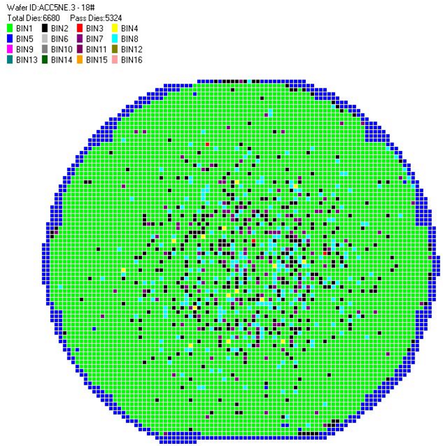
It is mainly divided into three ways: functional test, performance test and anti-aging test. It is mainly consisted of contact test, power consumption test, input leakage test, output level test, dynamic parameter test, analog signal parameter test and so on. Bad wafers are scrapped, which is called as black chip; some tests fail, but there is no problem for the use called as white chip, these can be sold out; and the Wafers all passed the test is positive chip.
13. Packing
Film the Wafer before inserting it into the black box.
14. Final test
The Die became the chip in our electronic digital products after final test.


Leave a comment