The development of solid state memory chip
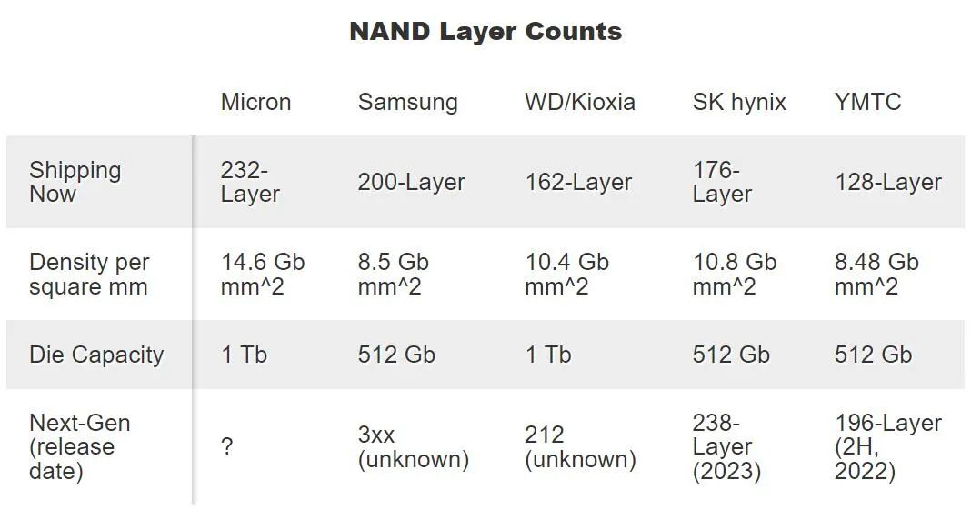
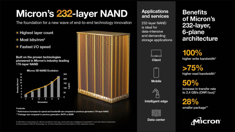
Major Solid state memory chip manufacturer Micron recently declared that scale production of its 232-layer NAND flash memory chip had begun. Therefore, solid-state memory chip in question is the first in the world to have more than 200 layers.
176-layer technology is now being offered by some rivals, and some competitors claim to be following pace. Probably some of them already have engineering samples with more than 200 layers.
New Micron Tech for Solid-state Memory
The new Micron tech as much as doubles the density of bits stored per unit area versus competing chips. It is packing in 14.6 gigabits per square millimeter. This density is between 35% and 100% higher than competitive TLC products. Moreover, it is roughly 43% higher than the company’s own 176L NAND.
The improved density has allowed Micron to finally produce their first 1Tbit TLC die. This is from a productization standpoint. Besides it, it means that Micron can now also produce 2TB chip packages by stacking 16 of their 232L dies. This is good news for SSD capacities, which at the high-end are often limited by the number of packages that can be placed.
Micron has been working on the size of their chip packaging at the same time. Even if the bigger capacity implies that their die size has grown generationally (we estimate 70.1mm2 given Micron’s density estimates), they nevertheless reduce the size of their chip packaging by 28%. A single chip package is consequently reducing from 12mm × 18mm (216mm2) to 11.5mm x 13.5mm (about 155mm2). This is fantastic news for Micron’s downstream clients.
How to enlarge the density?
Micron says they can store 1-terabyte chip in a 2-terabyte package. In this way, there is no more than a centimeter on a side, and can store around two weeks’ worth of 4K video (340 hours).
Besides density improvements, the latest generation of Micron’s NAND is also allowing the company to increase transfer speeds. The big news here is that Micron increases the number of planes within their NAND die from 4 to 6. Moreover, it is further improving the parallelism available within each die. Quad (four) plane designs become common in the previous generation of NAND. As the density of NAND grows, so the number of planes are for transfering rates to keep up with these greater densities. Micron confirm that the planes in 232L NAND offer independent reads.
This increase in parallelism, along with improved internal transfer rates, allow Micron to significantly improve their per-die read and write speeds. According to the company, read speeds improve by over 75% over their 176L generation NAND, and meanwhile write speeds have outright doubled.
In addition, Micron also emphasized that the 232-layer stack of 3D NAND Flash will consume less power than the previous generation. And it will have more energy-saving advantages when used in low-power products.
IDC estimates that in 2021, the world produced 81 trillion terabytes of data (or 81 ZB). And that by 2026, that amount will rise to 221 ZB. “Storage has to innovate to keep up,” said Alvaro Toledo, Micron’s vice president of data-center storage.
Update layers
The move to 232 layers is a combination and extension of many technologies Micron already deploy. To get a handle on them, you need to know the basic structure and function of 3D NAND flash. The chip itself is made up of a bottom layer of CMOS logic and other circuitry that is responsible for controlling reading and writing operations and getting data on and off chip as quickly and efficiently as possible.
Above teh CMOS are layers upon layers of NAND flash cells. Unlike other devices, flash-memory cells are built vertically. They start as a (relatively) deep, narrow hole etched through alternating layers of conductors and insulators. Then the holes are filled with material and processed to form the bit-storing part of the device. It is the ability to reliably etch and fill the holes through all those layers that is key limit to the technology. Instead of etching through all 232 layers in one go, Micron’s process builds them in two parts and stacks one atop the other. The new product’s 116 layers is higher than the previous generation’s 88 layers.
“It’s an astounding engineering feat,” says Alvaro. “That was one of the biggest challenges we overcame.”
According to Toledo, there is a path toward even more layers in future NAND chip. “There are definitely challenges,” he says. But “we haven’t seen the end of that path.”
Nand Flash Market
In addition, NAND flash makers are increasing the density by packing multiple bits into a single device. Each of the Micron chip’s memory cells is capable of storing three bits per cell. That is, the charge stored in each cell produces a distinct enough effect to discern eight different states. Though 3-bit-per-cell products (called TLC) are the majority, four-bit products (called QLC) are also available.
One QLC chip presented by Western Digital researchers at the IEEE International Solid State Circuits Conference earlier this year achieved a 15 Gb/mm2 areal density in a 162-layer chip. And Kioxia engineers even demonstrated a 7-bit cell last month at the IEEE Symposium on VLSL Technology and Circuits. However, it required dunking the chip in 77-kelvin (-196 degrees Celsius) liquid nitrogen. This unusually low temperature environment was chosen to reduce data read noise.
Micron is pitching 232L NAND as a full stack replacement for 176L NAND. It means that Micron considers it suitable for everything from mobile and IoT to PC and data center. According to Micron, its new NAND products, Crucial SSD devices, have already begun shipping to a select group of customers. Later this year, production of the new products will expand even more. And the new model SSD will be available in the market in a few months.
Micron has not announced any new Crucial products yet, which may mean that Crucial will deploy new NAND in existing products. So we need to pay attention to the performance of new products.
Reference:
https://spectrum.ieee.org/micron-is-first-to-deliver-3d-flash-chips-with-more-than-200-layers
https://www.anandtech.com/show/17509/microns-232-layer-nand-now-shipping
https://www.tomshardware.com/news/micron-takes-lead-with-232-layer-nand-up-to-2tb-per-chip-package
https://www.micron.com/products/nand-flash/232-layer-nand


Leave a comment