Latest Posts


Intel QLC SSD production exceeds 10 million!
Recently, Intel announced that its production of 3D NAND SSD based on QLC in Dalian plant since the end of 2108 has been over 10 million, marking another step towards QLC becoming a mainstream technology for mass storage.
Dave Lundell, director of SSD strategic planning and product marketing for Intel’s customers, said that many companies are talking about QLC technology, but Intel has achieved large-scale delivery. We have seen that the demand for cost-effective large-capacity QLC storage technology and Intel QLC storage solutions in the market is very strong.
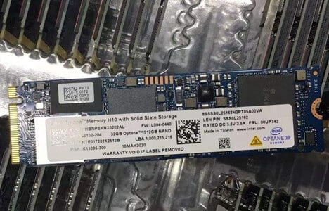
Currently, Intel QLC 3D NAND is mainly used in 660P series, 665P series and Optane Memory H10 storage solutions. Among them, it is worth mentioning that Optane Memory H10 is a “hybrid solid state disk” that integrates storage-grade memory (SCM) and NAND flash memory. Data that requires a low latency transfer rate is stored in the SCM, and data that does not require a low latency is stored in a NAND flash memory medium.
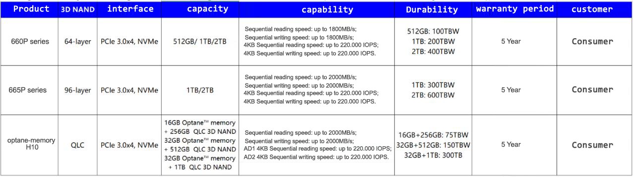
Image Source: webpage
Develop advantages and avoid weaknesses, QLC technology may shine in read-intensive applications
With the growing demand for high-density, large-capacity, high-performance storage devices in the market, major storage original equipment manufacturers have devoted all their effort to improve the storage density of each wafer. At the end of 2019, Samsung, Kioxia/ Western Digital, Micron / Intel, and SK Hynix have all achieved mass production of 90+ layer TLC 3D NAND, and have launched 90+ layer QLC products. According to previous media reports, Intel will launch 144-layer QLC 3D NAND this year.
With each upgrade of flash memory technology, the number of Dies produced by wafers of the same size is greater and the cost is lower. From 32-layer 3D NAND to 128-layer 3D NAND, the amount of GB per square has more than tripled, which is the main factor that drive the continuous growth trend of NAND Flash capacity.
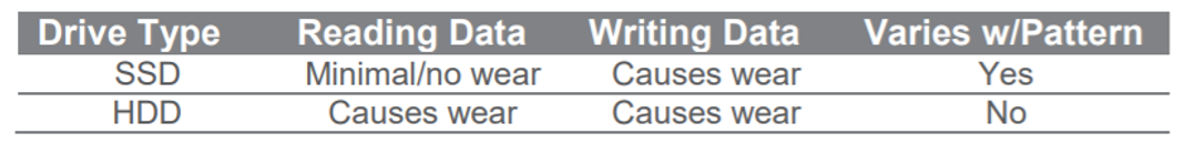
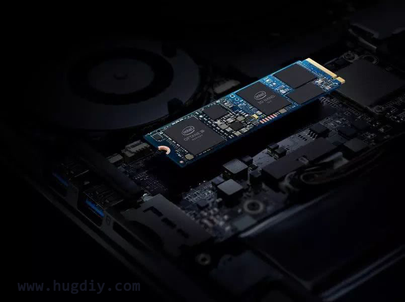
Image Source: webpage
Of course, although QLC technology can bring greater storage capacity and lower unit cost, it is questioned because of its poor stability and the P/E lifespan is only 1% of SLC’s, which is also an important reason that hinders its large scale popularity.
However, we have previously ignored a flash point of NAND Flash particles, that is, NAND Flash particles only wear when writing, and the wear caused by reading applications is insignificant. However, HDDs, which are currently the main media for mass storage, are subject to wear during both reading and writing process. Therefore, QLC technology has a unique advantage in read-intensive applications. In addition, the development of master control and error correction technology has further promoted the popularity of QLC.
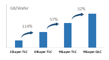
Image Source: webpage
In addition to Intel, Samsung, Micron and Western Digital also values the importance of the advantages of QLC in read-intensive applications. Micron and Western Digital have already sent QLC-related product samples to customers. Samsung has also built a comprehensive product line from Z-SSD to QLC SSD.
Continuously optimize storage architecture for higher density storage
Currently, the mainstream 3D NAND on the market are based on vertical channels and horizontally stacked gates. It Increases capacity through stereo stacking and has better performance and longer life. Under this architecture, it can be divided into floating gate architecture and charge trapping architecture according to different storage principles.
With the split of Intel and Micron, Intel may become the only practitioner of floating gate structures. Although Kioxia released the new 3D semi-circular split floating gate flash memory cell “Twin BICS Flash” in December last year, it still has no product output.
Intel introduced that in the past ten years, Intel has been developing QLC-related technologies. In 2016, the Intel R&D team changed the direction of the floating gate technology to vertical and wrapped it in the gate. This improvement brings the storage density of 3D TLC technology to 384 Gb/die. By 2018, 64-layer 3D QLC flash chips has become a reality, with a storage density of 1,024 Gb/die.
In a demand-oriented storage market, coupled with fierce competition among companies in the industry, more advanced technologies will definitely be developed. The 100+ layer stacked 3D NAND or QLC or even PLC technology are all meant to better meet the growing storage needs. With the advancement of 5G deployment, the Internet of Things, Internet of Vehicles, and artificial intelligence will release more market demand, and the storage market will also iterate out storage products with better performance and larger capacity. Let us wait and see!
Leave a comment