Latest Posts


How does the new X-NAND technology affect NAND Flash market?
News on November 15 During the three-day Virtual Flash Summit 2020, the CEO and founder of NEO Semiconductor, Xu Zhian (Andy Hsu), gave a definite speech to introduce the company’s new X-NAND flash memory structure. This is planning to combine the speed of SLC flash memory with the density and low price of QLC. Furthermore, it brings new chance for NAND Flash market.
NEO Semiconductor had started in San Jose, California in 2012 and has 20 memory patents. The company first disclosed its X-NAND technology in 2018. At that time, it was using as a storage solution for AI and 5G emerging markets. Now, they have shared more details about this technology.
Source: Tom’s Hardware, same below
Top performance from X-NAND
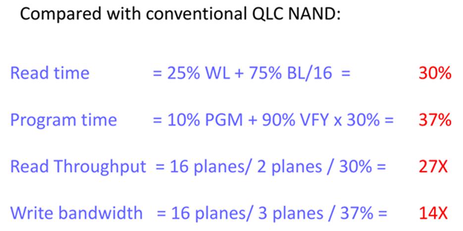
X-NAND promises to provide top performance: The company claims that its random reading and writing workload is 3 times faster than QLC flash memory. Moreover, it is 27 times/14 times faster in sequential reading and writing workloads respectively (see the above figure).
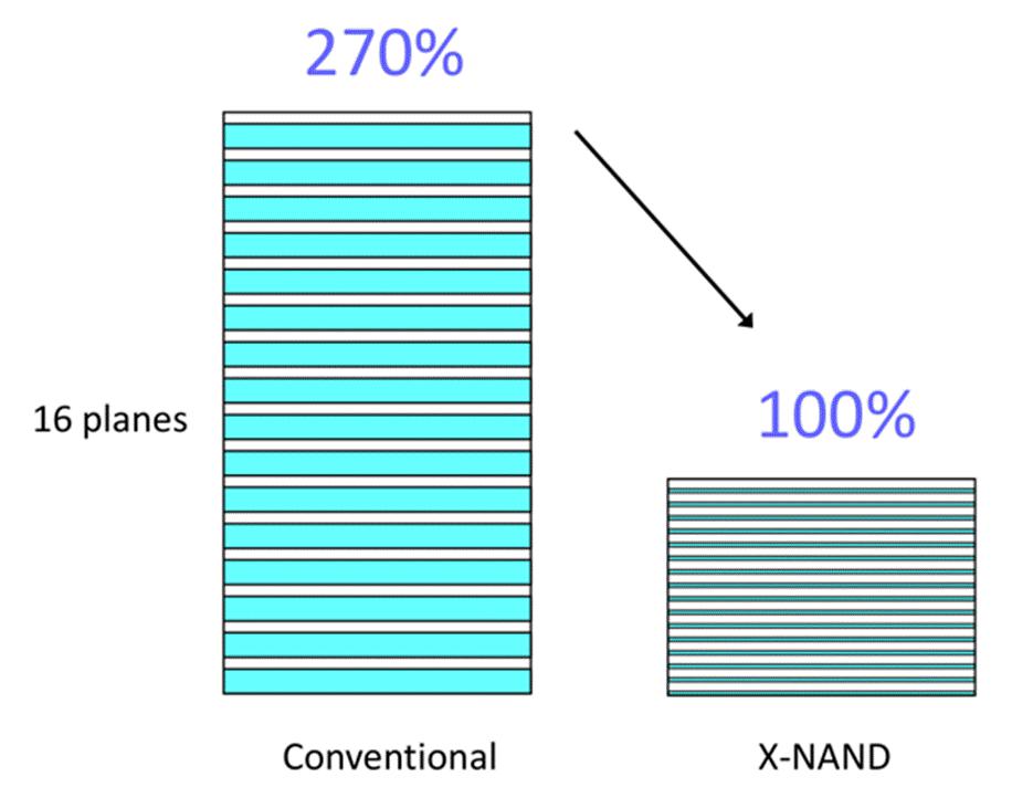
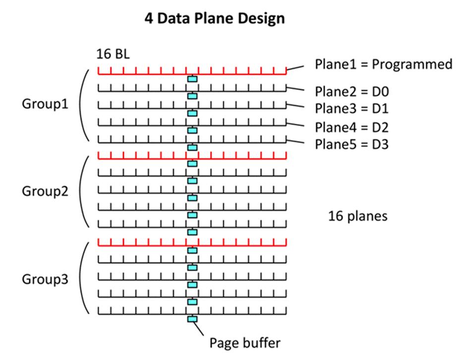
This is achieved by smaller die, which is approximately only 37% of the size of a 16-plane design (see the figure below). This can be flexible, and the chip size can be adjustable according to the speed.
Nevertheless, X-NAND still provides a rather high degree of parallelism even though its size is smaller. Just like in a smart phone or M.2 hard drive. The company also claims that this goal can be achieved without compromising durability or cost, and its power consumption is quite low.
The changes of NAND Flash market
As the NAND Flash market shifts to cheaper but slower flash memory to increase density (for example, from 3-bit TLC to 4-bit QLC), its performance and durability have essentially decreased, while its reading and writing latency has increased. This may reduce the sequential writing performance and has a huge impact on data center and NAS applications.
However, consumer-grade QLC hard drives rely heavily on SLC cache, which is composed of part of the local flash memory that operate in unit mode. But, it is difficult to have enough time for you to migrate writing data from SLC cache to the main QLC storage in enterprise workloads,.
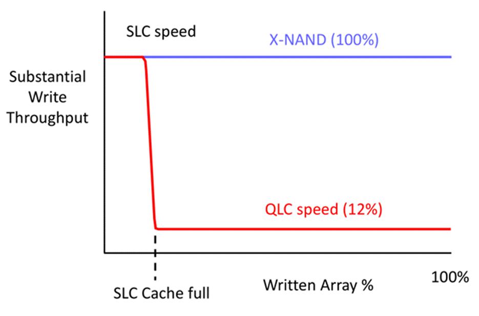
Instead, X-NAND provides a way for flash memory to maintain SLC performance through simultaneous conduct SLC and QLC writing modes (see the figure below).
Flash memory has a sharp increase
He pointed out that high-density flash memory is growing at an extremely fast rate. Because Western Digital will occupy 50% shares of QLC by 2024.
His goal for X-NAND is to ensure that it uses the traditional NAND process. At least the tradition structure remains the same, so there will be no additional costs. The whole process is running on the current NAND and uses fast sampling as a solution for development.
This strategy aims to accelerate the application of QLC, especially for data centers. Because the performance of flash no longer lags far behind I/O speed. In addition, the X-NAND programming and erasing strategy is to improve its endurance. Meanwhile, it makes its life longer than QLC flash memory (see figure below).
The characteristics of X-NAND in NAND flash market
X-NAND realizes these characteristics by changing the 16KB page cache of each plane to 1KB page. However, the size of the plane can be 16 times than the previous one.
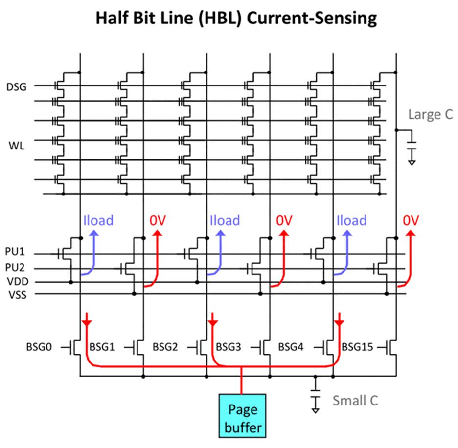
A plane is the smallest unit of flash memory, and each flash die has one or more planes. The page cache stores data in transmission between the bus and flash memory. Such as reading and writing data. The flash mode has planes in bit lines or cell strings (see the figure above). So plane division can reduce the length of the bit lines, which helps improve performance.
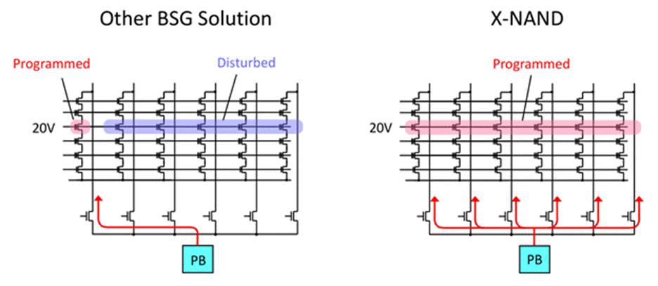
When X-NAND is in the reading or verifying process, the corresponding setup time can be reduced by block the adjacent bit line (see the figure below). This further enhances the technology and improves writing performance.
X-NAND has six main characteristics. There are multi-bit row writing, multi-plane QLC programming, program suspension, multi-bl reading, single-latch QLC reading, and the SLC/QLC parallel programming. Depending on the different implementation, this can greatly improve program. Because multiple planes can be using in the programming sequence.
Multiple memory units are used so that SLC and QLC programming can be realized at the same time. To ensure that the SLC page is never full, so QLC page can transfer data at the SLC speed. The program allows the use of internally shared inter-page cache data lines or I/O buses to minimize additional delays. Reading is improving by using plane to latch the reading of each bit line. Also, the data can be updating in a non-destructive way like DRAM due to the high capacitance.
Elinfor.com reminds that although the vision is very good, it may still take a long time to implement this technology in real life.
Leave a comment