Latest Posts


Yangtze Memory officially released 128-layer TLC/QLC flash memory chip
As the epidemic situation in China has stabilized, Wuhan, the epicenter, has been officially unblocked recently. How will the Yangtze Memory show up after more than 70 days of blockade? Will the 128-layer 3D NAND be extended? Can the monthly production capacity of 100,000 pieces be fulfilled as scheduled?
Faced with industry chain concerns, Yangtze Memory released two 128-layer 3D NAND products on April 13th, namely: 128-layer QLC 3D NAND flash memory with a capacity of 1.33Tb and 128-layer TLC 3D NAND flash memory with a capacity of 512Gb, among which the 128-layer QLC product is currently the industry’s first NAND flash memory with a die capacity of 1.33Tb. Its capacity and performance are better than those of its main competitors, and both products have been verified by mainstream controller manufacturers. In addition, it also responded to external concerns.
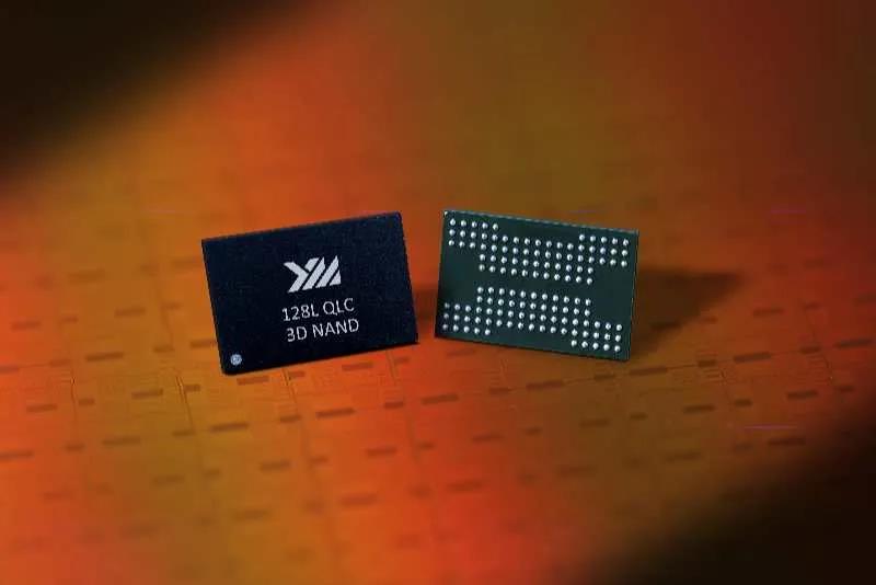
Yangtze MemoryX2-6070 128L QLC 1.33Tb NAND Flash
Source: Yangtze Memory
With the industry’s highest storage density, highest I/O transmission speed, and the highest capacity of a single die, this memory “newcomer”, who is less than 4 years old, is not easy
Yangtze Memory 3D NAND is based on Xtacking® innovative technology, which can realize the optimal combination of control circuit and storage unit, so that the product has relative advantages in storage density, I/O performance and reliability. The core innovative technology Xtacking® used in the newly released 128-layer series of products, has been fully upgraded to 2.0, further releasing the potential of 3D NAND flash memory.
Regarding the Xtacking®2.0 architecture, Yangtze Memory Co-Chief Technology Officer Tang Qiang said that the advantages of Xtacking®2.0 are mainly reflected in three aspects: “The first one is higher I/O speed, which is currently implemented on 128-layer products. The second one is that we can customize the design of CMOS wafers and partners because Xtacking®2.0 CMOS wafers and array wafers are developed and manufactured separately. The third one is that we can add functions that are more beneficial and helpful to the system on CMOS based on Xtacking® structure. ”
In terms of I/O reading and writing performance, both products can achieve a data transmission rate of 1.6Gbps at 1.2V VCCQ voltage, which is the highest in the industry. Coupled with a single die capacity of up to 1.33Tb, Yangtze Memory’s 128-layer QLC flash memory products can be said to be better than industry’s main competitors. At the same time, it also proves to the industry that the Xtacking® architecture is forward-looking and mature.
For the test results of the two products, Yangtze Memory also said that the SATA solid state drive equipped with Yangtze Memory QLC 3D NAND was installed as the system disk into the win 10 system for boot test. The boot speed was 12-15s, which was a good achievement in the engineering sample stage.
Gong Yi (Grace), Senior Vice President of Marketing and Sales of Yangtze Memory, said: “As a newcomer in the flash memory industry, Yangtze Memory has achieved a leap from 32 layers to 64 layers to 128 layers in just 3 years. This is a huge achievement for all employers in Yangtze Memory and is also the result of collaboration between the upstream and downstream of the global industrial chain. With the advent of the Xtacking® 2.0 era, Yangtze River Storage has the determination, strength and ability to create a new business ecology so that our partners can fully use their own advantages to achieve mutual benefit and win-win. ”
The Yangtze Memory 128-layer NAND flash memory will start mass production at the late first half of next year. In the future, it will cooperate with 100,000 pieces of monthly production capacity when it is in full opreation, and will play a key role in balancing global supply.
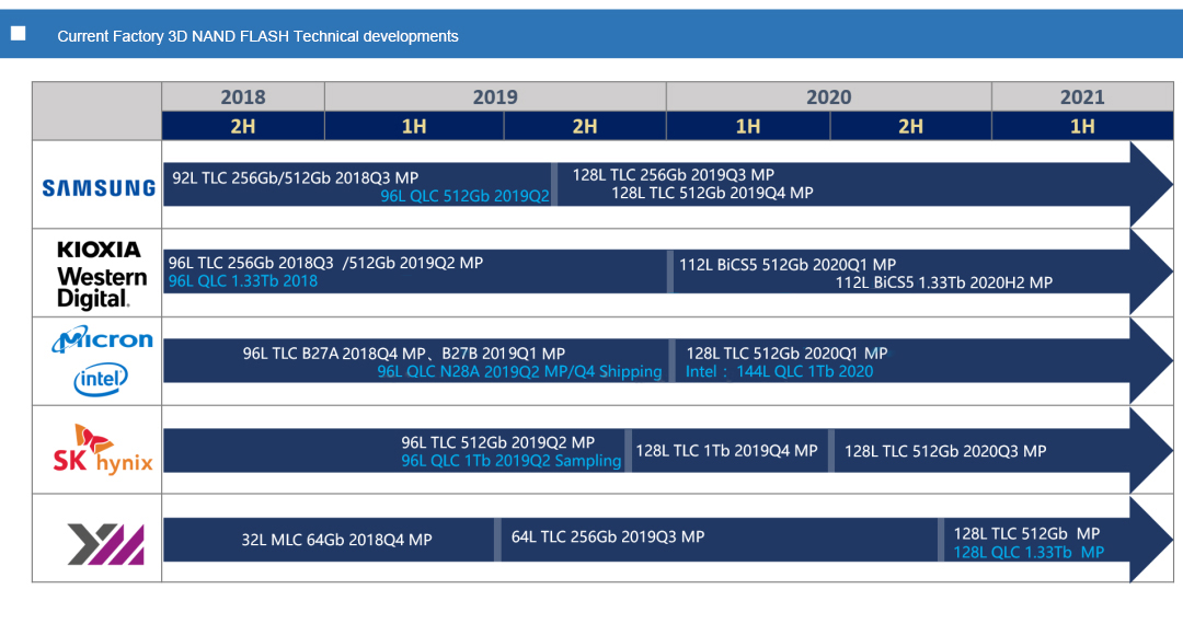
As we all know, the NAND Flash industry is a highly cyclical industry that is extremely sensitive to the supply and demand balance and has fierce cost competition. In 2019, the main production capacity of major manufacturers has switched from 64/72-layer NAND Flash to 92/96-layer stacked NAND Flash. According to China Flash Market data, global bit shipments in 2019 increased by 35% to 309 billion GB from 2018.
Source: ELINFOR Flash Market
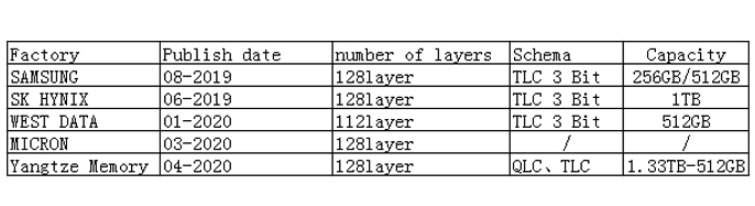
At present, Samsung, SK Hynix, Kioxia/Western Digital have successively released the latest 100+ layer 3D NAND products. Among them, Samsung announced in August last year that it has mass-produced 250GB SATA SSDs based on this technology, and in November, mass production of the sixth generation 128-layer 512Gb TLC 3D NAND was achieved. SK Hynix has delivered engineering samples of 12layer 1Tb 4D NAND to its major costumers in November 2019, and recently announced the launch of an enterprise SSD based on the first 128 layer 1Tb TLC 4D NAND flash memory. Kioxia/Western Digital also announced the joint development of 512Gb BiCS5 TLC in January this year. The sample came out in the first quarter of this year. They also plan to launch 112-layer 1Tb (128GB) TLC and 1.33Tb QLC products.
Since Micron’s “breakup” with Intel, the two parties have become independent after 96-layer 3D NAND technology and second-generation 3D XPoint technology. Recently, in its second quarter online meeting, Micron also pointed out that it plans to start mass production of 128-layer 3D NAND based on a new architecture in the third quarter of this year and start commercial shipments in the fourth quarter, but the specific product details are not specified. On the other hand, Intel has reported that it plans to launch 144-layer 3D QLC NAND technology this year. There is no official information released by both parties yet, but the market is looking forward to it.
As a rising star, Yangtze Memory has successfully mass-produced 64-layer 3D NAND since September last year, and became the first domestic storage manufacturer in China to successfully introduce its customer base. After 7 months, the industry-leading 128-layer 3D TLC/QLC NAND Flash was released, making it compatible to mainstream manufacturers in the industry.
Regarding the capacity ramping and yield issues that is concerned by the industry, Yangtze Memory stated that it is still gradually promoting according to the established goals, and is expected to achieve 100,000 monthly production capacity by the end of 2020 to 2021. Currently, 64-layer products have reached the level of mainstream manufacturers in consumer-grade products, and will launch eMMC, UFS, and SSD products based on 64-layer 3D NAND in the second half of this year. Subsequent launches of enterprise-level and PC OEM and other product yields will be further improved.
In addition, Yangtze Memory further stated that the main mass production time of 128-layer products should be from the end of this year to the first half of next year.
In terms of application market, Gong Yi introduced: “Yangtze Memory 128-layer products will bring greater value to partners and have broad market application prospects. Among them, the 128-layer QLC version will be the first to be applied to consumer-grade solid state drives, and Gradually enter enterprise-level servers, data centers and other fields to meet the diverse data storage needs of the future 5G and AI era. ”
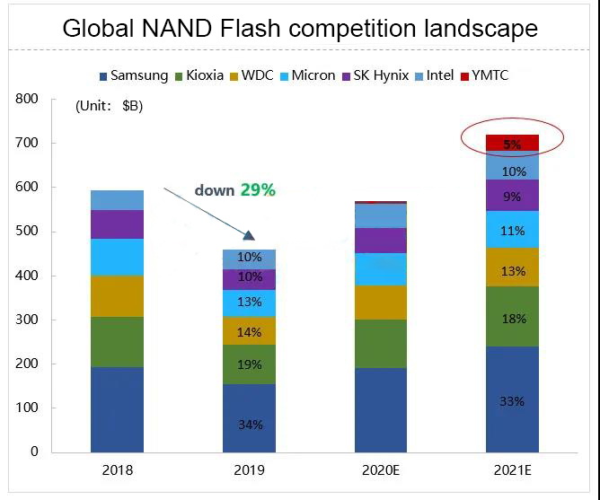
Under the impact of this year’s epidemic, major manufacturers’ financial performance is under pressure, they strategic prioritize supply in of data centers, mobile phones and PC OEM markets, resulting in tight supply in the channel market. Although Yangtze Memory occupied for less than 1% of the total market in 2019, with the gradual improvement in production capacity, the market occupation is expected to account for 5% by 2021, which will effectively balance the global flash memory market supply pattern.
Source: ELINFOR Flash Market
In fact, major OEMs have eagerly launched mass storage solutions in 2020, because the value the upcoming large-capacity mobile storage, data center and enterprise-level storage demand driven by 5G in 2020. Although the sudden emerged epidemic disrupted the original market pace early this year, in the long run, the upward and better trend of the storage market remains unchanged, and the demand will still exists, but it is only delayed.
QLC technology with higher storage density and more cost advantages will shine in read-intensive applications
With the increasing demand for high-density, large-capacity, high-performance storage devices, major storage manufacturers have spared no effort to increase the storage density of each wafer. In addition to increasing the number of stacked layers on the three-dimensional architecture, increasing the number of bits stored in each storage unit is also an important direction of improvement.
Therefore, the QLC technology has received more and more attention from the original factory due to its larger storage capacity and lower unit cost. However, its poor stability and its P/E lifespan in only one percent of SLC’s made it be highly questioned, and is also an important reason for hindering its large-scale popularization.
Source: Internet
With the in-depth study of NAND Flash, it was found that NAND Flash particles will only wear when writing, but the wear caused by reading applications is negligible. Therefore, QLC flash memory products can make full use of the characteristics of NAND Flash, combined with its high density and cost-effective advantages, it plays a unique advantage in read-intensive applications. In addition, the development of master control and error correction technology can also help make up for the birth defects of QLC.
Among the major OEMs, Intel is the most active one in promoting QLC technology, and QLC has been widely used in 660P series, 665P series and Optane Memory H10 storage solutions. According to reports, Intel plans to launch the next-generation 144-layer 3D NAND based on QLC architecture first, and then TLC architecture products will be launched later. Micron also announced the first QLC-based 5210 SATA SSD, which has been certified by most major server OEMs.
In addition, Kioxia/ Western Digital also plans to launch a 112-layer 1.33Tb QLC product, and Samsung has also built a comprehensive product line from Z-SSD to QLC SSD.
Yangtze Memory follows the mainstream of the industry and is the first to launch QLC flash products with a single die capacity of 1.33Tb. It also emphasizes the huge market potential of QLC technology in read-intensive applications with higher storage density and more economical cost advantages.
Regarding the cost competitiveness of 128-layer QLC, Gong Yi said that when QLC was first launched at 64-layer or 96-layer, its cost advantage was not so big compared with TLC. As its density becomes higher, the cost advantage will become more significant.
For major manufacturers, 2019 can be described as struggling. It was originally expected that through the popularity of 5G in 2020, server demand will drive shipments, but the sudden epidemic has disrupted the established rhythm, and profits may continue to be delayed. Since new comers like Yangtze Memory are working hard to catch up the mainstreams, achieving 100+ advanced craftsmanship, has doubled the pressure of which major manufacturers face. However, for the major manufacturers who have been through so many difficulties, these pressures will eventually be transformed into the driving force to provide the market with products with higher capacity and better performance.
Leave a comment