Latest Posts
What is MLC NAND Flash Memory?
MLC and SLC are two different types of NAND FLASH memories. They can be used as the storage media for MP3 players, mobile hard drives and other products.
Content
- A brief introduction
- The characteristics
- The shortcomings
- The status quo
MLC(Multi-Level Cell)
A brief introduction
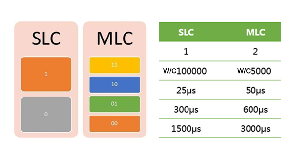
SLC needs to be referred to to explain about MLC. SLC is the acronym of single-level cell, or single level cell flash memory. And the full name of MLC is multi-level cell, or multi-level cell flash memory. The difference between them is that each unit of SLC can only store one bit of data, while each unit of MLC can store two bits of data. The data density of MLC is twice that of SLC.
According to the above explanation, MLC is more powerful because of its higher density. MLC is also better in terms of cost. Many chip makers have changed from SLC to MLC. In August 2006, Samsung officially changed from SLC to MLC. In October 2006, Samsung began mass production of MLC flash chips. Samsung chip’s number starts with K9G, and the the number K9L refers to MLC. Hyundai chip’s number starts with HYUU, and HYUV is for MLC. The characteristics
SLC is characterized by high cost, small capacity and fast speed, while MLC has a larger capacity and low cost, but slow speed. Each unit of MLC is of 2bit, which is twice as many as that of SLC. However, the probability of error increased thanks to the larger data storage in a MLC unit and its relatively complex structure. The error correction must be carried out, which leads to its performance falling significantly behind the SLC that has a simple structure. Meanwhile, the advantage of a SLC chip is its rewrite number can reach up to 100,000, which is 10 times higher than that of a MLC chip. To ensure the life of a MLC chip, the control chip has the checksum intelligent wear balance algorithm, so that the write times of each storage unit can be shared equally, reaching 1 million hours of mean time between failure (MTBF).
The shortcomings
MLC has its advantages and disadvantages.
Deficient write and read performance
Compared with SLC, MLC has a deficient write and read performance. SLC can read and write about 100,000 times, while MLC can only read and write about 10,000 times. And some MLC products can even reach only about 5,000 times.
Slow speed
Under the same conditions, the read and write speed of MLC is slower than that of SLC. The speed of a MLC chip is only about 2m.
High power consumption
Under the same conditions, MLC consumes about 15 percent more power than SLC.
This is because of the change of the MLC system, which requires the support of new control chips. With some MP3 products and USB drives still using the old design, the MLC chips may go awry with data loss, slow transmission speed and other defects. The fact that a large number of SD cards were called back in 2006 due to their using MLC chips while there was not the support of new master chips has had many ramifications. The status quo
MLC chips are used more and more widely after Samsung and Toshiba started their mass production. The increased storage density of the new MLC chips set a higher bar for main control chips. Digital devices such as digital players and flash drives that read and write frequently increase the error probability of the MLC chips. For applications such as video and audio, it is necessary to have control chips and ECC verification mechanism. At present, some main control chips have only passed the software verification, which virtually increases the burden of the main control chips. Some main control chips have passed the combined 4bitECC hardware verification and software verification, so as to reduce the burden of the main control chips. But this can only help reduce the probability of error to a certain extent. The disadvantages of MLC, such as chip write limit and transfer speed, are insurmountable.
MLC is superior to SLC in architecture. Many manufacturers have done a lot of optimized development of MLC. They may continue such development, though with technologies that are not so mature. In terms of cost, MLC chips are cheaper than SLC chips. That is why many manufacturers have chosen MLC chips to go with the original architecture while not using control chips or ECC verification. That has resulted in many problems, with many people calling such MLC chips fakes. So, we can’t only look at the prices but need to think more careful when purchasing MP3s, USB drives or other digital products.
MLC technology began becoming popular in February 2003 when Toshiba launched its first MLC architecture NAND flash products. As the leading manufacturer of NAND flash products at that time, Samsung Electronics paid little attention to this architecture and went its own way vigorously promoting the SLC architecture. In April the following year, Toshiba again successively launched the 4GBIT and 8GBIT NAND flash chips using MLC technology. Obviously, this added to the strength of its NAND flash products that already have a large capacity.
Samsung Electronics for a long time advocated the SLC architecture, claiming that it is superior to MLC. But the ISSCC papers on MLC technology published by the company in 2004 and 2005 initially showed a change of its view. Samsung did not at that time provide any marketing materials about MLC flash memory products on its website. But it had developed a 4GBIT MLC NAND flash memory chip. Its die area is 156mm2, which is 18mm2 larger than that of Toshiba’s 90nm process MLC NAND flash memory chip. The competition between the two major NAND flash chip manufacturers on MLC architecture was heating up. Apart from Samsung and Toshiba, there was the IM technology company which, with the Intel MLC technology, also wanted to surpass its competitors in technology and MLC quality. The MLC technological competition went into full swing.





Leave a comment