Latest Posts


NEO Semiconductor creator of X-NAND Gen2 technology.
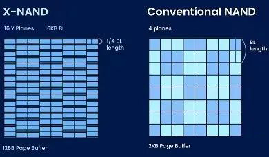
NEO Semiconductor, a leading developer of innovative architectures for NAND flash and DRAM memory, is the creator of X-NAND technology. The whole point of X-NAND is to divide the plane of the memory matrix into 4-16 so-called planes, each of which can be interacted with in parallel, to speed up IO. Recently, the company revealed the new X-NAND Gen-2, which doubles throughput over X-NAND Gen1.
X-NAND has six primary features: multiple bit line writes, multi-plane QLC programming, program suspend, multi-BL reads, single latch QLC reads, and the aforementioned SLC/QLC parallel programming. Depending on the implementation, this can improve program throughput substantially as multiple planes can be used in the programming sequence.
The use of multiple banks allows for simultaneous SLC and QLC programming, ensuring the SLC pages are never full, while data can be programmed to the QLC pages at SLC speed. The program suspect function enables using the internally shared inter-page buffer data lines or I/O bus to minimize additional latency. Reads are improved by having a plane latch the read per bit line, with DRAM-like refreshing of data in a non-destructive way due to high capacitance.
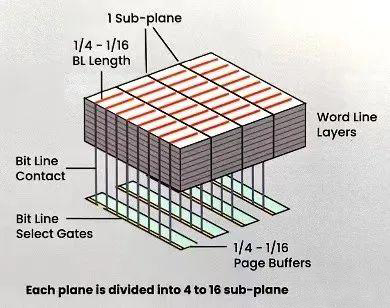
The technology takes a base NAND die with two to four access planes. Each plane is divided into four to 16 sub-planes, each accessed in parallel. Page buffers are used to optimize data throughput speeds. A brochure explains that with gen 1, a total of four planes are used for SLC/TLC parallel programming. Input data is programmed into three SLC word lines in three planes and then programmed to a TLC word line in a fourth plane.
Gen 2 X-NAND does things differently. Two planes are used for SLC/TLC parallel programming. Input data is programmed into three SLC word lines, as before, but now only in one plane, and then programmed to a TLC word line in a second plane. This enables data writes to occur in parallel with fewer planes, and X-NAND delivers SLC-like performance from larger capacity and lower cost QLC memory.
X-NAND gen 2, says Neo Semiconductor, delivers 3,200MB/sec of sequential write throughput, 20x faster than a basic SSD. There are also unspecified latency improvements.
It also provides 3x the base random read/write speed and there is zero increase in die size.
X-NAND architecture supports SLC, MLC, TLC, QLC and PLC variants of NAND. The IP can be deployed by NAND manufacturers (Kioxia, Micron, Samsung, SK hynix, Solidigm, Western Digital, and YMTC), and is compatible with current technologies and processes with zero increase in manufacturing cost. At least this is the pitch by Neo Semiconductor.
So far, we haven’t heard of any NAND manufacturers using Neo’s X-NAND technology.
Neo Semiconductor also has an X-DRAM technology, based on shorter bit lines and reduced capacitance, which adds parallelism. This, it says, increases DRAM performance with 400 percent refresh data throughput, lowers the voltage needed, and reduces overall power consumption.


Leave a comment