Latest Posts


DRAM is mostly used for main memory, and SRAM is mostly used for cache. Non-volatile storage are commonly used in sd card、USB Flash and SSDs.
All users must be familiar with the term “memory”, because all electronic products must use memory, and they usually use more than one type of memory. However, many people are quite confused when it comes to memory types, specifications, and formats, such as NAND Flash, which is so expensive recently, DRAM that is often mentioned in industry news, and SRAM, SDRAM, DDR 3, DDR 4, NOR Flash… What are these products?
ARAM can make SDRAM, DDR, NAND Flash can make Micro SD Card、SD card 、USB Flash drive、 SSD.
People who are not familiar with PC knowledge often ask question when buying equipment, such as what is the difference between hard disk and internal storage? My hard drive already has 1TB capacity, but why the PC still runs very slowly?
The difference between hard disk and internal storage is that whether data can still be saved safely after the power is turned off. Even if the power is turned off, data saved in hard disk will not disappear.
But when we want to calculate data, it will take too long if the CPU wants to directly grab data from the hard disk. So ” internal storage” will act as an intermediate bridge. First, internal storage copies data from the hard disk, and then let CPU directly take the data from the internal storage for calculation. This will be millions of times faster than grab data directly from the hard disk.
The processing speed of the internal storage is much faster than that of the hard disk, but data will disappear when the power is cut off, and the price of the internal storage is more expensive than that of the hard disk.
Of course, there are more details in the memory hierarchy. Please see the content below.
To put it simple, there is also a storage space in the CPU called Register. When calculation is required, CPU loads the data from the internal storage into the register, then perform calculation with the number stored in the register, and then stores the result back into the internal storage after the calculation. After all, CPU and internal storage are still two different chips, it can’t be as fast as grab data from the same piece of chip.
Another concept is Cache, which is an intermediate bridge between CPU and internal storage.
In terms of speed, inside CPU, it is: Register> Cache> internal storage > hard Disk. The higher the level (closer to the CPU), the faster the speed, the higher the price, and the lower the capacity.
Classification of memory
Electronic memory refers to the memory that read and write with electricity. It is mainly divided into two categories, as shown in Figure 1:
Volatile Memory (VM): Data exists when the power is turned on, and losts immediately when the power is turned off (data evaporates), such as SRAM, DRAM, SDRAM, DDR-SDRAM, etc.
Non-Volatile Memory (NVM): Data exists when the power is turned on, and data can still be kept when the power is turned off, such as ROM, PROM, EPROM, EEPROM, Flash ROM, FRAM, MRAM, RRAM, PCRAM, etc.
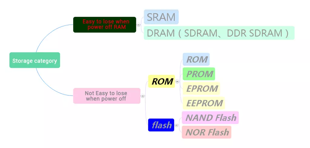
▲ Figure 1: Classification of memory.
The cell of memory
The “cell” of the memory refers to the smallest structure used to process data. If it contains one transistor and one capacitor, it is called “1T1C”; if it contains one transistor and one resistor, it is called “1T1R”; if it contains one diode and one resistor, it is called “1D1R”.
Each “cell” of the memory may not only store 1 bit of data. As our requirements for memory capacity are getting higher and higher, each “cell” can store more and more data. According to the number of data each “cell” can store, memory is further divided into: Single-Level Cell (SLC), Multi-Level Cell (MLC), Triple-Level Cell (TLC), and Quad-Level Cell (QLC) etc.
Memory hierarchy
To understand the various memory configurations of electronic products, we must first introduce the concept of “Memory hierarchy”. The memory hierarchy refers to how to properly allocate a variety of memories with different capacities, different computing speeds, and different unit prices, in order to achieve the greatest economic benefits, so that the product’s computing speed, storage capacity, and the product price are all reasonable.
Figure 2 is a diagram of the memory. From top to bottom, there are register, cache, main memory, and assistant memory:
Register: Inside the processor, it is used to set the function of the processor, mainly to set the value of “temporarily store”.
Cache memory (also known as cache, cache area, etc.): Inside the processor, this is the place where programs and data are “temporarily stored” when executing programs, usually made of SRAM.
Main memory: Outside the processor, the place where programs and data are “temporarily stored”, usually made of DRAM, but has now been improved to SDRAM or DDR.
Assistant memory: outside the processor, where programs and data are “permanent stored”, including: flash memory, disk drives, optical drives, tape drives, etc.
Different types of storage have different capacity, working speed, and unit price.
Storage capacity: assistant memory (GB)> main memory (MB)> cache memory (KB)> register (B).
Working speed: assistant memory (1ms)
Unit price: assistant memory
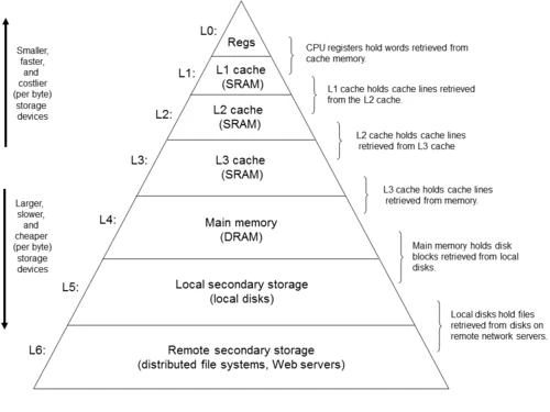
▲ Figure 2: Diagram of memory hierarchy.
Memory application
All electronic products must use memory, and usually use more than one type of memory. Due to the wide variety of memory, users are often confused. We briefly explain the differences between different memories. Figure 3 shows the system block diagram of the main chips of mobile phones. It includes: application processor, baseband processor, motion controller.
The application processor mainly executes the operating system (OS) and application program (App). The register and cache memory are currently built in the processor, and the register is used to set the function of processor. The software program that is used to set the value of the register, and to motivate the hardware is also called “firmware”. The cache memory is used to “temporarily store” the program. Since it is relatively closer to the arithmetic unit in the processor, so it can shorten the time to transfer program and data and speed up the execution of the program, therefore, it is called “Cache”.
Because of the cost of the cache memory is pretty high, its capacity is not large. When there is not enough space when executing the program, you can put it in the main memory instead. However, the current SDRAM or DDR used in the main memory is a volatile memory. It will lose data immediately after shutting down power, so data must be stored in non-volatile assistant memory after shutdown. Early assistant memory uses disk drives, optical disc drives, tape drives, etc. Due to the progress of semiconductor manufacturing processes, most of them now use Flash ROM or the so-called solid state disk (SSD). Solid state disk is actually made of flash memory as well.
Since the cache memory (SRAM) and the main memory (SDRAM, DDR) are used to “temporarily store” programs and data when executing programs, they are directly connected to the computing unit in the processor by a bus, their capacity is measured by “Bit”. The assistant memory is a place to “permanently store” programs and data it generally used “byte” to calculate capacity since a byte can store a half-type word.
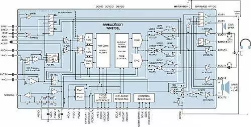
▲ Figure 3: System block diagram of the main chips of mobile phones.
Static random access memory (SRAM: Static RAM)
6 MOSs are used to store 1 bit of data, and there is no need to periodically replenish the power supply to maintain the memory content during use, so it is called “Static”.
The structure of SRAM is quite complicated (6 MOSs to store 1 bit of data). Its access speed is relatively fast because it does not use capacitors, but the cost is also higher. Therefore, it is generally made into memory that require lower capacity but higher speed, such as the built-in 256KB, 512KB, 1MB “Cache memory” in central processing unit (CPU) , they generally use SRAM.
Dynamic Random Access Memory (DRAM: Dynamic RAM)
A MOS plus a capacitor is used to store one bit of data, and DRAM “need” periodical power replenish to maintain the memory content during use, that is why it is called “Dynamic”.
The structure of DRAM is simpler (one MOS plus one capacitor). The access speed is slower due to the longer time required for charging and discharging the capacitor, but the cost is also lower. Therefore, it generally made into memory that requires higher capacity but lower speed. For example, DDR-SDRAM with more than 1GB usually used on the motherboard of a personal computer is a kind of DRAM. As the speed of the processor is getting faster and faster, the speed of traditional DRAM can no longer meet the requirements, so it is now improved into two types of SDRAM or DDR-SDRAM for use.
Synchronous Dynamic Random Access Memory (SDRAM: Synchronous DRAM)
The central processing unit (CPU) and the main memory (SDRAM) on the motherboard have same “clock” when accessing data, so it is called “synchronous”. Since CPU does not need to “wait” when accessing data, it is more efficient. SDRAM has a faster access speed than DRAM. So early computer motherboards used SDRAM to replace traditional DRAM, but there are a few industry computers that still use SDRAM at present.
You can remember a simple conclusion: SRAM is faster, DRAM is slower; SRAM is more expensive, and DRAM is cheaper.
This is the internal storage we usually use in our computers. More precisely, it should be called “Memory Module”. A memory module is actually composed of a small circuit board plus a few DRAM chips. There are a total of 8 DRAM chips on the memory module in the picture above. Let’s take a look at the internal structure of a DRAM chip, we will see a memory array.
CPU will give this storage array a “row address” and a “column address”, so a “storage unit” can be selected. Common storage unit includes 4 bit or 8 bit, and each bit uses a circuit structure. We call it a “basic storage unit” of DRAM.
This basic storage unit contains a transistor and a capacitor. Then the current memory state can be told by whether the capacitor is charged or not.
The action of “write on memory” is done by to charge or discharge the capacitor with an external data line and write down digital data of 1 or 0.
DRAM uses a MOS and a capacitor to store ine bit of data (a 0 or a 1), as shown in Figure 4 (a), when the MOS is not conducting, no electrons can went through and the capacitor has no charge, representing the data of this bit is 0, as shown in Figure 4(b); when the MOS is conducting (a positive voltage is applied to the gate), electrons will flow from the positive side to the negative side, and the capacitor will have charge, which represents the data of this bit is 1. In order to “store” the charge went through, a tiny capacitor must be used as shown in Figure 4(c). DRAM is slower than SRAM because its capacitor takes time to charge.
▲ Figure 4: Ddiagram of the structure and working principle of dynamic random access memory (DRAM).
Since capacitor may leak electricity, resulting memory loss due to insufficient potential difference. Therefore, unless the capacitor is charged periodically, there is no guarantee that the data can be stored for a long time.
Since the circuit structure of each DRAM basic storage unit is very simple, the power consumption is low and the price is low too. Therefore, DRAM chips with large storage capacity can be manufactured at low price. The disadvantage is that the reading and writing speed is slow (because the capacitor needs to be charged and discharged), which affects the performance of DRAM.
The structure of SRAM is more complicated, with a total of six MOSs. We can mark them with M1, M2, M3 to M6 respectively. These six MOSs can only store one bit together.
SRAM chips are different from DRAM chips. They do not need to be divided into row addresses and column addresses. The design of SRAM is relatively more flexible. The number of storage units corresponding to an address can be 8 bit, 10 bit, 32 bit, 40 bit or 64 bit.
In addition, the switching speed of the MOS is much faster than the charging and discharging speed of the capacitor, so the reading and writing speed of SRAM is much faster than that of DRAM.
However, six MOSs are used to store one bit in SRAM. The area of the chip inevitably becomes larger as the number of MOSs increases, which made it harder to make the integrated circuits smaller and its price is more expensive.
(The price of SRAM is more than 1000 times higher than that of DRMA. For example, in the 2010 generation — SRAM’s storage price per unit is $60/MB, and DRAM’s is only $0.06/MB.)
Also, every MOSs consumes power. The more MOSs, the higher the power consumption. Considering the higher price and higher power consumption, SRAM is only be used in some very demanding places, such as the cache mentioned above.
Therefore, currently the “main memory” still uses DRAM technology, but the small “cache” used to increase operating speed uses SRAM. However, whether it is DRAM or SRAM, the stored data will be lost if power is turned of, so they are all called volatile memory.
Ferroelectric Random Access Memory FRAM
Dynamic Random Access Memory (DRAM) uses a MOS plus a capacitor to store one bit of data. Since traditional DRAM capacitors use “silicon oxide” as an insulator, the dielectric constant of silicon oxide is not large enough (The K value is not large enough), so it is not easy to attract (store) electrons and holes, which makes it necessary to constantly replenish electrons and holes, that is why it is called “dynamic”. Once the computer power is turned off, the electrons and holes stored in the capacitor will be lost, and the data stored in DRAM will also be lost.
To solve this problem, the easiest way is to use a material with a large enough dielectric constant (large enough K value) to replace the “silicon oxide” as an insulator, so that electrons and holes can be stored in the capacitor without losing. At present, the industry uses “lead zirconate titanate” (PZT) or “strontium bismuth tantalum” (SBT), a “ferroelectric material” with large dielectric constant (large K value) to replace silicon oxide. It can store electrons and holes without losing, so that the originally “volatile” dynamic random access memory (DRAM) becomes “non-volatile” memory, and is called “ferroelectric random access memory” (Ferroelectric RAM, FRAM).
What is NAND Flash
Let’s continue to talk about the non-volatile part:
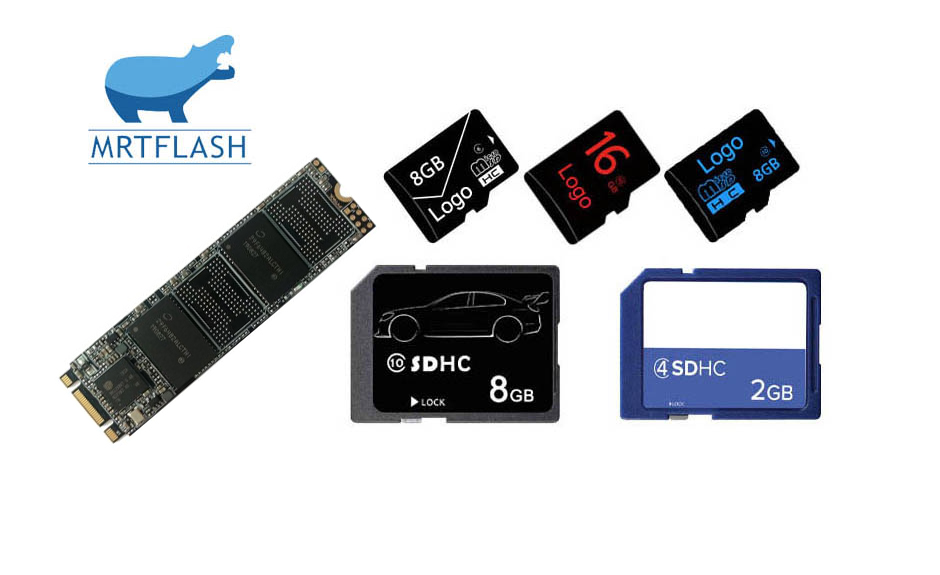
Flash are light weight, small size, and consumes low power. it is used in the hard disk of various electronic products. NAND Flash can be divided into NOR-type Flash and NAND-type Flash. Can make Micro SD 、SD card 、USB Flash Drive 、SSD.
NOR Flash was introduced into the market earlier than NAND Flash. The reading speed is faster, but the writing speed is slower and the price is more expensive than NAND Flash.
NOR Flash is currently used to store the program code of the operating system or important data, such as used in ROM. For example, the Taiwanese manufacturer Macronix, which produces NOR Flash, has entered the ROM supply chain of the Nintendo Switch console, and its revenue have increased greatly this year.
NAND Flash has faster writing speed and lower price, so NAND Flash is currently the most commonly used one. NAND Flash is the mainstream technology used in current USB hard drives and mobile phone storages.
In addition, Solid State Drive (SSD) is also a storage device based on NAND Flash. SSDs are not like traditional hard disks (HDD), which have parts such as motors and read-write arms. HDD’s speed is slow, the power consumption is high, and it is very sensitive to vibration, so it is difficult to use in small mobile devices.
SSD has no noise when reading and writing data. It is shock-resistant, fast in transmission, and can be reduced to a weight that is less than one-tenth of the weight of HDD. It has now become the mainstream storage device for personal computers and laptops.
Summary
According to whether the data can be retained when the power supply is off, storage can be divided into “volatile” and “nonvolatile” storage. Volatile storage is divided into DRAM and SRAM.
SRAM is faster but more expensive, so DRAM is mostly used for main memory, and SRAM is mostly used for cache.
Non-volatile storage is divided into ROM and Flash. Mainly used as a hard disk.
Flash is divided into NOR Flash and NAND Flash. Hard disks are mostly SSD composed of NAND Flash nowadays.
Leave a comment