Latest Posts


All major events affect the storage industry in 2020
2020 is an is an extraordinary year for the storage industry. In the first half of the year, the industry suffered a hit by the “epidemic” and the international trade war. In the latter half of the year, a substantial rise in semiconductor chip price was affecting by the shortage of foundry production, and led to an dramatic fluctuations in the storage industry.
Although the storage industry faces greater challenges, nothing can stop the advancement of the storage industry. In order to respond to market changes better, Samsung, Kioxia, Western Digital, SK Hynix and other original manufacturers are making new changes and breakthroughs in investing, technology, and strategy aspects.
Storage Industry: SK Hynix and Micron have successively break through 176-layer 3D NAND technology
In 2020, Samsung, Kioxia, Western Digital, Micron, SK Hynix, etc. all devoted in promoting 9x-layer 3D NAND in the market. At the same time, Samsung 1XX layer, Western Digital/Kioxia 112 layer, SK Hynix 128 layer, Micron 128 layer, and Intel 144 layer 3D NAND continue to increase their production proportion, and actively promote their application in SSD products.
At the end of 2020, Micron and SK Hynix made public announcement that they have made the very first breakthroughs in 176-layer 3D NAND. Micron announced in November that the company would start mass production of the world’s first 176-layer 3D NAND Flash. Its reading latency and writing latency will be improving by more than 35%. The maximum data transmit rate is 1600 MT/s, which has increased by 33%. The mixed workload performance has increased by 15%, the compact design reduces the die size by about 30%, and each wafer will produce more GB equivalent of NAND Flash.
4D NAND Flash from SK Hynix and Samsung
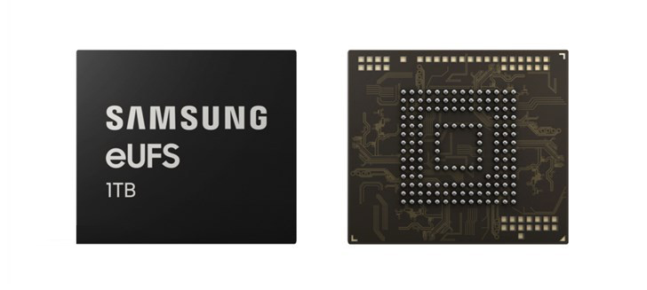
SK Hynix however, announced the launch of 176-layer 4D NAND in December. Comparing with the previous generation, its Bit productivity has increased by more than 35%. Furthermore, its reading speed has increased by 20%, and data transmission speed has increased by 33% to 1.6Gbps. Later, 1Tb-capacity 4D NAND based on 176-layer will also emerge. Basing on the new 176-layer 4D NAND technology, UFS and SSD products are ready to show up in mid-2021.
In addition, Samsung also announced that it will start mass production of the seventh-generation V-NAND in 2021, using “dual stack” technology. The number of stacking layers has not been disclosed yet. However, at its 128-layer production phase, Samsung uses “single stack” technology to produce 3D NAND. Samsung also emphasized that the use of “dual stack” technology not only can make its product technically more competitive, but also might make 3D NAND to stack up to 256 layers. But this does not necessarily mean that Samsung’s seventh-generation NAND will adopt this configuration.
DRAM technology: first introduce Samsung 1Znm to EUV, and the original factory will enter a new stage of 1αnm technology in 2021
In 2020, Samsung, Micron, SK Hynix and other DRAM technologies will mainly make progress from 1Ynm to 1Znm. This is also the third-generation 10nm-level technology of DRAM. When it comes to the fourth-generation of 10nm-level, EUV processes will be introduced on a large scale.
In 2020, Samsung’s mass-produced 16Gb LPDDR5 introduced EUV technology for the first time. Based on the 1Znm process technology, its capacity has increased by 33% compared to 12Gb, and the package is also 30% thinner, thanks to the more advanced technology. At the same time, Samsung also plans to start mass production of 16Gb DDR5/LPDDR5 based on the fourth-generation 10nm-class (1α) EUV process in 2021.
Micron has increased the output of 1Znm LPDDR5 and is promoting the continuous innovation of GDDR6X. At the same time, the 1αnm DRAM, which is still in the research and development stage, will be mass-produced in the first half of 2021. With a mature yield rate, the 1αnm process node will increase the number of bits per wafer by 40% compared to the 1Znm node.The 1βnm process is in the initial development stage.
SK Hynix plans to promote the mass production of the fourth-generation 10nm class (1a) DRAM by using the advantages of EUV technology. At the same time, it is going to start mass production of 1a nm DRAM in the beginning of 2021.
Investment and plant construction: Samsung Xi’an Phase II, Pingze P2, Kioxia K2, Fab7, etc.
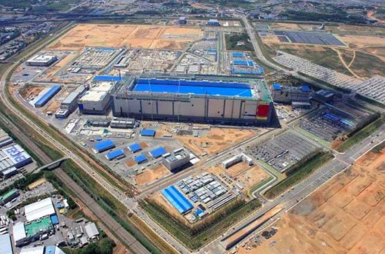
Under the competition in the storage industry, investment is an essential part. In 2020, Samsung will start the first phase production in China Xi’an’s second phase factory. The second phase of the production in the second phase factory will be completed in the latter half of 2021. At the same time, the Pingze P2 plant will invest 8 trillion won to build a new NAND Flash production line. It plans to start production in the latter half of 2021. And Samsung plans to build a new P3 factory.
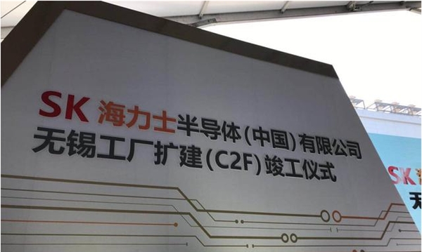
Kioxia and Western Digital had invested the new K1 plant in Kitakami, Iwate Prefecture. The new plant had begun small-scale production in the first half of 2020. On the north side of the Yokkaichi memory production base, the Fab7 plant land is under construction. The construction consists of two phases. The first phase of construction will finish in the spring of 2022. Besides it, Kioxia also announced that it will expand its production base in Iwate, Japan. It will expand its K2 plant next to the existing K1 plant. The construction is going to start in the spring of 2021 and be ready in the spring of 2022.
Micron status in storage industry
Micron is building a new A3 factory clean room. It is estimated to start mass production of 1Znm or 1α technology in 2021. At the same time, Micron also plans to apply for the construction of the A5 factory project in 2021 and continue to invest in DRAM. This factory will adopt the miniature technology after the 1Znm process, to further expand the scale of mass production of advanced technologies. As for SK Hynix, the Ichuan M16 factory will launch chips in the first half of 2021 and make shipments in the latter half of the year.
Yangtze Memory’s second phase memory base project has also officially started construction. The total investment to the national memory base project has reached 24 billion US dollars. There are two phases for 3D NAND chip factory. The first phase has started construction in the end of 2016, and has achieved a production capacity of 100,000 pieces/month. The planned production capacity of the second phase is 200,000 pieces/month, and the monthly production capacity of the two phases will be 300,000 pieces.
Strategic adjustment: major structural changes in the original factory will trigger global turbulence
1. Samsung’s senior personnel transfer in storage industry
In December 2020, Samsung made changes to the company’s management. Five Samsung executives experienced personnel changes, and three of them got a promotion.
In addition, Samsung did not arrange personnel for the chairman of the company. It is still vacant.
2. Western Digital integrates Flash and HDD technical resources to establish an independent product business department
Western Digital has integrated Flash and HDD technical resources and has established an independent product business department in order to provide diversified storage product portfolio solutions, which will enable SSD and HDD product lines to be more flexibly scheduled, learn from each other’s strengths, and meet market needs better.
3. Kioxia postponed its original IPO plan in 2020, and Toshiba wants to sell its Kioxia shares
Because the market has continued its turbulence in and the uncertainty brought by the outbreak of the “epidemic”, Kioxia has postponed its original listing plan on October 6, 2020, and will continue to evaluate the appropriate time for listing. Industry insiders believe that if Kioxia misses the deadline in February 2021, its IPO plan will be postponed to the latter half of 2021.
It is worth mentioning that Toshiba, as one of Kioxia’s shareholder, expressed that it no longer has intention to engage in memory-related businesses, and announced that it will sell some of its common stocks of Kioxia in August 2020.
4. SK Hynix integrates the two major development departments of DRAM and NAND Flash in storage industry
At the end of 2019, SK Hynix announced that it will conduct a series of personnel transfers and business reorganizations in 2020. It includes integrating the two major development departments of DRAM and NAND Flash together. The aim is to achieve unified management from development, manufacturing, and business post-processing. After the reorganization, Jin Kyo-won, the chief semiconductor technology expert of SK Hynix, will be promoted to the president of development and manufacturing. He will be responsible for DRAM and NAND Flash from development to mass production, and to improve operational efficiency.
SK hynix announced in 2020 that it will invest 55 million US dollars to establish a Gauss laboratory. What’ more, it will realize manufacture innovation through industrial AI solutions.
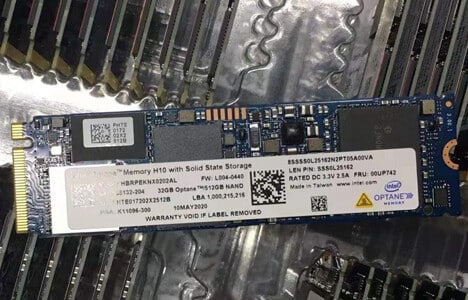
5. Intel sold its NAND business and Dalian factory to SK Hynix
After Intel ended its NAND Flash technology cooperation with Micron, they sold their shares in joint venture factory to Micron. And then it solds its NAND business to SK Hynix, including the Dalian factory in China that produces 3D NAND.
According to the agreement, Intel’s NAND SSD business and NAND factory will be handed over to SK Hynix. However, the transaction still needs approval from regulatory. At the same time, Intel will continue to produce NAND wafers in the Dalian plant. In addition, it retains all intellectual property rights. This is relating to NAND wafer manufacture and design until the transaction gets complete in March 2025. This production structure is to protect the legal ownership of intellectual property rights.
Leave a comment