Latest Posts


JEDEC Solid State Technology Association released the final specification of DDR5 SDRAM standard today
The JEDEC Solid State Technology Association will release the final specification of its next mainstream memory standard DDR5 SDRAM today, which will mark an important milestone in the development of computer memory. Since the late 90s, the latest version of DDR has been driving the development of PCs, servers and all other products. DDR5 has once again expanded the capabilities of DDR memory, doubling the peak memory cards speed and greatly increasing the memory size.
It is expected that by 2021, hardware based on the new standard will begin to be adopted at the server level, and then extended to client PCs and other devices.
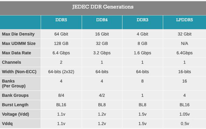
The DDR5 specification was originally planned to be released in 2018. Today’s release is a bit behind JEDEC’s original plan, but it does not reduce the importance of the new memory specification. Like each iteration of DDR before, the main focus of DDR5 is once again to improve memory density and speed. JEDEC hopes to double both, the maximum memory speed is set to be at least 6.4Gbps, and the capacity of a single packaged LRDIMM will eventually reach 2TB.
For long, there have been some minor changes to support these goals or simplify certain aspects of the ecosystem, such as voltage regulators on DIMMs and ECC on chips.
Getting bigger: denser memory and chip stacking
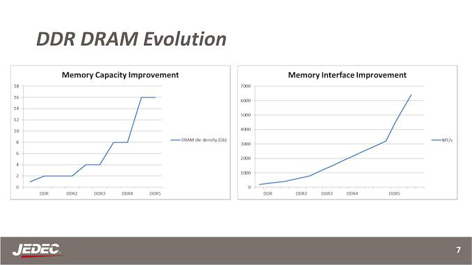
Firstly, we shall briefly introduce the capacity and density, because compared with DDR4, this is the most direct change to the standard. The designing time of DDR5 is several years, and it allows a single memory chip to reach a density of 64Gbit, which is 4 times higher than the maximum density of 16Gbit of DDR4. Combined with die stacking, it can stack up to 8 die into one chip, so a 40-unit LRDIMM can reach an effective storage capacity of 2TB. Or for the more inconspicuous unbuffered DIMM, this means that we will eventually see a DIMM capacity of 128GB in a typical dual-rank configuration.
Of course, when chip manufacturing catches up with the range allowed by the specification, the peak capacity of the DDR5 specification will be used in the later part of the standard’s life cycle. First, memory manufacturers will use today’s attainable density 8Gbit and 16Gbit chips to build their DIMMs. Therefore, although the speed increase of DDR5 will be quite immediate, as the manufacturing density increases, the increase in capacity will be slower.
Faster: one DIMM, two channels
Another part of DDR5 is that it increases memory bandwidth again. Everyone wants higher performance (especially with the growth of DIMM capacity), and it is not surprising that a lot of work has been done in the specification to achieve this goal.
For DDR5, JEDEC hopes it start working more aggressively than the DDR memory specification. Usually, the new standard starts from where the previous standard ended, such as the transition from DDR3 to DDR4. DDR3 officially stopped at 1.6Gbps, and DDR4 started from there. However, for DDR5, JEDEC’s goal is higher. The organization is expected to start at a speed of 4.8Gbps, which is about 50% faster than the official 3.2Gbps maximum speed of DDR4. In the following years, the current version of the specification will allow data rates of up to 6.4Gbps, twice the official peak level of DDR4.
Of course, enthusiasts will notice that DDR4 has exceeded the official maximum of 3.2Gbps (sometimes much higher), and DDR5 may eventually follow a similar route. Regardless of the specific number, the basic goal is to double the available bandwidth of a single DIMM. Therefore, don’t be too surprised if SK Hynix does achieve the DDR5-8400 target later in this decade.
The basis for these speed targets is changes on the DIMM and memory bus to feed and transfer large amounts of data every clock cycle. As with DRAM speed, the biggest challenge comes from the lack of progress in DRAM core clock rates. The special logic special logic circuit is still getting faster and faster, and the memory bus is getting faster and faster, but the clock frequency of the capacitor and transistor-based DRAM that supports modern memory still cannot exceed a few hundred megahertz.
Therefore, in order to get more benefits from the DRAM die (to keep the illusion that the memory itself is getting faster and provide the memory bus that is faster than actual one), more and more parallelism is required. DDR5 raises the stakes again.
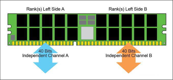
In fact, the biggest change here is similar to what we have seen in other standards such as LPDDR4 and GDDR6, a single DIMM is broken down into 2 channels. DDR5 does not provide a 64-bit data channel for each DIMM, but provides two independent 32-bit data channels for each DIMM (40 bits when considering ECC). At the same time, the burst length of each channel is doubled from 8 bytes (BL8) to 16 bytes (BL16), which means that each channel will deliver 64 bytes per operation. Compared with DDR4 DIMMs, DDR5 DIMMs that runs twice the rated memory speed (same core speed) will provide two 64-byte operations within the time that the DDR4 DIMM transfers one DDR4 DIMM, thus doubling the effective bandwidth.
Overall, the magic number for memory operations is still 64 bytes, because this is the size of a standard cache line. The larger burst length on DDR4 style memory can bring 128-byte operations, which is too large for a single cache line, and if the memory controller does not want to occupy the value of two lines of preface data, this will lead to efficiency/utilization loss. In contrast, since the two channels of DDR5 are independent, the memory controller can request 64 bytes from different locations, which makes it more suitable for the actual working method of the processor and avoids utilization penalty.
In this way, the ultimate impact on standard PC desktops will be to replace today’s DDR4 plan, that is, two DIMMs fill two channels for 2×64-bit settings, and DDR5 systems will function as 4×32-bit settings. The memory will still be installed in pairs – we will not go back to the era of installing 32-bit SIMM – but now the minimum configuration is two of the smaller channels of DDR5.
This structural change will also have a knock-on effect in other places, especially to maximize usage in these smaller channels. DDR5 introduces a more fine-grained memory bank refresh function, which will allow some memory banks to be refreshed while in use. This allows the necessary refresh (capacitor charging) to be performed faster, thereby maintaining waiting time and making unused storage banks available as soon as possible. The maximum number of memory bank groups has also increased from 4 to 8, which will help reduce the performance loss caused by sequential memory access.
Fast Bus Service: Decision Feedback Balance
Compared to finding a way to increase the number of parallelization of DRAM DIMMs, increasing the bus speed is both simple and difficult: this idea is simple in concept but difficult to implement. Ultimately, to double the memory speed of DDR, the operating speed of the DDR5 memory bus must be twice that of DDR4.
DDR5 has made several changes to achieve this goal, but surprisingly, the storage bus does not have any large-scale fundamental changes, such as QDR or differential signaling. Instead, JEDEC and its members have been able to achieve their goals with a slightly modified version of the DDR4 bus, even though this bus must operate within tighter tolerances.
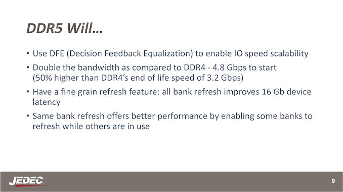
The key driving factor here is the introduction of Decision Feedback Equalization (DFE). At a very high level, DFE is a method of reducing inter-symbol interference by using feedback from the memory bus receiver to provide a better equalization effect. Better balance can also make the DDR5 memory bus operate at a higher transfer rate and at required clearer signal transmission without any failure. At the same time, some minor changes in the standard further help this, such as the addition of new and improved training modes to help DIMMs and controllers compensate for small timing differences on the memory bus.
Simpler motherboard, more complex DIMM: voltage regulation on DIMM
With changes in core density and storage speed, DDR5 once again increases the operating voltage of DDR memory. According to the specifications, the Vdd of DDR5 is 1.1v, which is lower than the 1.2v of DDR4. Like past updates, this will improve the power efficiency of memory relative to DDR4, although so far, the power consumption has not improved as much as DDR4 and earlier standards.
JEDEC also introduced voltage regulation method of DIMMs in the DDR5 memory standard to make very important changes. In short, voltage regulation is moving from the motherboard to individual DIMMs, and DIMMs are responsible for their own voltage regulation requirements. This means that DIMMs will now include an integrated voltage regulator and are suitable for everything from UDIMMs to LRDIMMs.
DDR5 DIMM: still 288 pins, but the pinout has been changed
Finally, as has been widely proven in early supplier prototypes, DDR5 will maintain the same 288-pin count as DDR4. This reflects the transition from DDR2 to DDR3, where the number of pins remains the same at 240 pins.
However, don’t expect to use DDR5 DIMMs in DDR4 slots. Although the number of pins has not changed, the pin arrangement has adapted to the new features of DDR5, especially its dual-channel design.
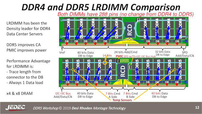
The biggest change here is that the command and address bus is shrunk and partitioned, and its pins are reassigned to the data bus of the second storage channel. DDR5 will have two 7-bit CA buses instead of a single 24-bit CA bus, one for each channel. Of course, 7 is only half of the old bus, so things are getting more and more complicated for the exchanged storage controller.
Send samples now and start using them in the next 12-18 months
Like other JEDEC specification released, today’s release has fewer products, and more standards set by the development committee for its members to use. Major memory manufacturers who have been involved in the DDR5 development process from the beginning have developed DIMM prototypes and are now considering packaging them to bring their first commercial hardware to the market.
The overall adoption curve of DDR5 is expected to be similar to earlier DDR standards. In other words, JEDEC expects that DDR5 will begin to appear in terminal devices within 12 to 18 months after the hardware is completed, and increase from there. Although the group did not provide specific product guidance, they made it very clear that they hoped that servers would once again become a driving force for early adoption, especially in large and very large-scale products. Neither Intel nor AMD has officially announced the use of new memory platforms, but it is only a matter of time at this point.
Meanwhile, they expect the life cycle of DDR5 to be as long as DDR4, or even longer. Both DDR3 and DDR4 enjoy a life cycle of about 7 years, and DDR5 should have the same stability. Moreover, although it is not possible to see several years ahead clearly, at this time JEDEC believes that due to the continuous maturity of the technology industry, the guarantee life of DDR5 will be longer than that of DDR4. Of course, this is the same year that Apple abandoned Intel’s CPU, so by 2028, everything is possible.
No matter what, as DDR5 is ready for release, you can expect major memory manufacturers to continue to show off their prototypes and commercial DIMMs. With the official start of adoption in 2021, it seems that next year will bring some interesting changes to the server market and ultimate client-end desktop market.
Leave a comment